
Controlled Impedance on High-Speed Flex PCBs
By ZM Peterson • Dec 18, 2024Flex PCBs can support controlled impedance routing normally found in high-speed PCB design thanks to a hatched ground plane.
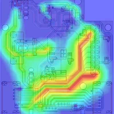
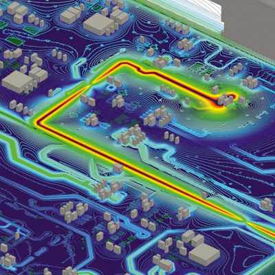
Data rates and required channel bandwidths in modern electronics are only going one direction: up! That's why signal integrity in digital and RF designs continues to become more important in a range of products. Today's digital processors are fast enough that just about every PCB must incorporate best practices for signal integrity. As designs get more advanced, the depth of signal integrity analysis and simulation only increases. This is why advanced electronics companies collaborate with NWES to solve their toughest signal integrity challenges and improve their designs.
In high‑speed PCB and substrate systems, signal integrity issues go far beyond simple reflections or crosstalk; challenges include frequency‑dependent dielectric loss, inter‑symbol interference (ISI), substrate parasitic coupling, power plane resonances introducing jitter, and dielectric anisotropy affecting impedance and propagation velocity. Our services integrate EM modeling, channel analysis, and eye diagram simulations to assess signal behavior from the substrate to the PCB, addressing performance defects before fabrication.
Signal impairment often stems from nuanced physical factors: dielectric loss in high‑bandwidth channels; coupling via shared dielectric layers; impedance shifts in anisotropic multilayer PCB stackups; and PDN resonances that degrade timing and increase bit error rates. We provide stackup and material validation, signal integrity analysis in both time and frequency domains, and calibrated eye‑mask evaluation across board and substrate layers. This enables precision tuning of design parameters, improving waveform fidelity, timing margin, and interconnect resilience in demanding high‑speed systems.
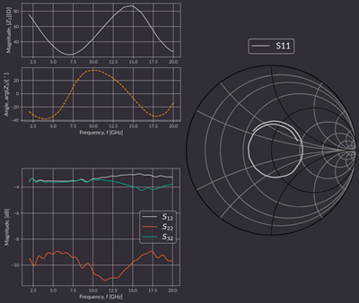
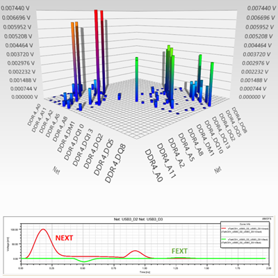
Fast analysis and full 3D electromagnetic simulation of PCB interconnects for standardized interfaces, such as PCIe, USB, DDR, and Ethernet.

System-level EM and PI/SI solvers for PCB interconnects, IC substrates, and chip-to-board signal integrity and power delivery.
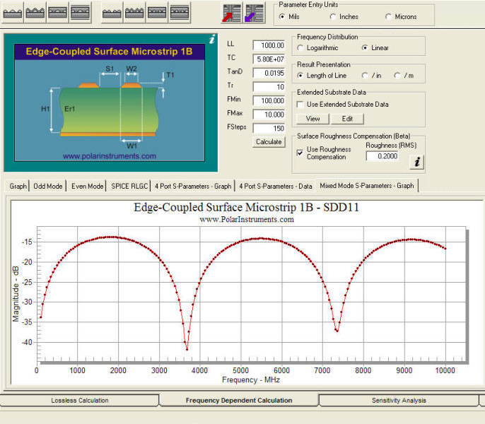
Paired field-solver and stackup planning to achieve controlled impedance with reliable manufacturability at the beginning of a new design.
High-frequency 3D EM analysis for complex geometries, enclosures, high-speed digital designs, and RF designs.
Open-source time-domain and frequency-domain solver for any 3D geometry with tools for rapid validation of digital and RF designs.
Before moving to fabrication, a detailed review of SI-related metrics provides crucial insight into channel performance; we help you quantify integrity risks and drive confident design decisions.
When design prototypes reveal issues like high-frequency attenuation, excessive dispersion, or eye closure, targeted revisions are essential. We review your design using advanced simulation tools and we then recommend updates that restore signal integrity before prototyping.

We offer PCB design services for a range of products, spanning high-speed digital systems, power systems, aggressive form factors, and RF devices. Upon completing a design review, we provide a detailed report outlining the required changes and a quote for the design updates. We use industry-standard enterprise-level PCB design software for all client projects.

![]()

Flex PCBs can support controlled impedance routing normally found in high-speed PCB design thanks to a hatched ground plane.

Differential pairs require a measurement reference, which could be a PCB ground plane or the other trace in the pair.

Learn how to choose the best PCB design software for your high-speed PCB design projects.


