
Differential pairs have a single geometric design parameter that changes the routing rules used in high-speed PCBs. This parameter is the spacing between the traces in the pair. Spacing influences how much of one trace's return path propagates in the other trace. The result is that the two traces can act as references for each other, reflecting the fact that a signal is measured between the two traces in the differential pair.
It is often asked, is ground needed to route differential pairs with a defined impedance? Technically, ground is required for a differential interface to recover some signal from a differential pair. However, in certain conditions on a PCB, you won't be able to design useful differential pairs without ground. In other cases, such as on a cable, there is no ground, and yet the interface still works as designed. This article will explore the various situations involving differential pairs without ground, including reaching into the ultra-high-density interconnect (UHDI) design regime where traces are spaced very close together.
Differential Pairs Can Function Without Ground
A differential pair is normally used for serial interfaces when suppression of common-mode noise and low electromagnetic field strength around the pair are priorities. These are characteristics of EMI/EMC and illustrate one of the main reasons differential interfaces were originally developed: to reduce radiated emissions around cable runs for high-speed digital interfaces being routed between telecom equipment.
This situation, with a cable between two devices, is illustrated below.

Differential pairs can be routed across a cable without requiring a ground wire.
Many protocols function this way, with the most notable example being Ethernet over copper twisted pair. Clearly, differential pairs can function in this interconnect, and the reason is that each trace acts as a voltage reference (a.k.a. ground) for the other trace.
One reason differential pairs are used in this way is that it eliminates the need to bridge grounds across the cable, thus you could have two isolated ground with some voltage offset between them. Differential interfaces take the difference between the two signals, thus they can survive any DC voltage offsets between the two regions. These voltage offsets can be quite large, reaching 10 V as measured in the lab by Dr. Howard Johnson (see his SigCon website for more information).
A PCB Ground Plane Helps Determine Differential Pair Impedance
The differential impedance of a differential pair is determined mainly by four factors:
- The distance to ground planes or coplanar copper pours
- Dielectric constant of the PCB substrate materials
- Spacing between the traces in the differential pair
- The copper weight of the etched copper foil
If you remove the ground plane from a differential pair in a PCB—whether it's coplanar or a dedicated ground plane—this will impact the geometry needed to achieve a target differential impedance. Because all signal integrity metrics begin with impedance, this will also affect the rest of your signal integrity metrics at different frequencies.
When discussing single-ended transmission lines on a PCB, we often refer to the return current. This is the capacitive coupling of a displacement current from a signal into the ground plane due to the transmission line's self-capacitance. Because differential pairs are also coupled transmission lines, they require a return current. This is a key point to understanding what happens with differential pairs that do not have a ground plane. We can then examine other signal integrity and EMI factors, such as radiated emissions and differential crosstalk.
Where Is the Return Current?
When the topic of routing a differential pair without a ground plane (e.g., over a cable) comes up, someone will inevitably ask where the return current exists for each side of the differential signal. The options are:
- In the neighboring trace
- In the ground plane
- In the trace and the ground plane simultaneously
The third answer is correct. This explains why you can route differential pairs without having them right next to each other (so-called tight coupling), or you can route them onto a cable with copper twisted pair. As long as the copper interconnect has the correct impedance and bandwidth, the interface can still function.
In a simple approximation, the return current distribution beneath each trace is roughly Gaussian. The image below shows this rough distribution; it is an image I often show in seminars and one of my articles on Altium resources.
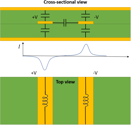
Differential pairs have some return current in a nearby ground plane.
The amount of return current in the opposite polarity trace or plane does not significantly affect signal integrity. What matters is the electric and magnetic field lines around the differential pair, as these field line distributions determine the amount of crosstalk in a differential pair.
A Ground Plane Affects Differential Crosstalk
The presence or absence of ground near a differential pair also determines the amount of mutual capacitance and mutual inductance with respect to another interconnect. These factors influence the amount of crosstalk a differential pair can inject into another trace or the amount it can receive. This is one of the most important reasons to use ground planes near differential pairs, particularly as serial data rates increase. Because ground near a differential pair allows for larger spacing for a target trace width, it also impacts the ratio of differential-mode to common-mode noise when crosstalk occurs in a differential pair.
A simple way to see this is by examining the electric and magnetic field lines between two differential pairs. Specifically, when we look at two differential pairs side-by-side, it's clear that the distance to ground and spacing between pairs will determine the magnetic flux that generates inductive crosstalk. The same idea applies to electric flux.

Electric and magnetic field lines around a differential pair.
How does this change when there is no ground plane on the PCB or no ground wire on a cable? The amount of crosstalk generated or received in a differential pair will only depend on the spacing between the traces and their impedance. This is why twisted pair wiring is so effective for controlling crosstalk in cables, even when there is no ground wire or shielding: the spacing between the wires is essentially zero.
Fine Linewidth and Coplanar Ground
Tightly coupled lines with very low spacing, such as in HDI or UHDI PCBs, can have strong enough electric and magnetic field coupling that the impedance can hit an interface target without the lines being excessively large. This can also be done without a ground plane on the next layer, or rather with a ground plane much farther from the traces than is typical in a high-speed PCB. Another instance is with coplanar ground, where a copper pour on the same layer as the differential pair sets its impedance to the target value.
The approach with copper pour is most common in two-layer boards that have a differential interface. For example, USB 2.0 can be routed up to the high-speed spec at the required differential impedance of 90 ohms by using coplanar copper pour.

Access this project on our PCB Design Examples page or on the dedicated project page.
In the above image, the USB lines are routed on a 2-layer PCB, but the same can be done on a single-layer PCB with no plane on the back layer. The 2-layer USB module shown above can be accessed on our Example PCB Projects page.
Whether you use fine-line routing with small spacing or coplanar ground, the lack of a solid ground plane will impact radiated emissions and EMI susceptibility in products requiring immunity testing. If EMI becomes a problem and leads to failure, the simple solution is to add ground back into the PCB stack-up.
Whether you're designing high-speed PCBs for mil-aero embedded systems or a complex RF product, you should work with a design and development firm that can ensure your product will be reliable and manufacturable at scale. NWES helps aerospace OEMs, defense primes, and private companies in multiple industries design modern PCBs and create cutting-edge embedded technology, including power systems for high reliability applications and precision control systems. We've also partnered directly with EDA companies and advanced ITAR-compliant PCB manufacturers, and we'll make sure your design is fully manufacturable at scale. Contact NWES for a consultation.
Ready to start your next design project?
Our Clients and Partners


