


Meet Your
PCB Design Experts
Since 2017, we've provided electronics design and PCB design services to large OEMs, SMBs, and startup technology companies. Our designers have a broad range of experience working in industries such as military & aerospace, embedded systems/IoT, industrial electronics, drones, and robotics. We also work directly with EDA software companies providing design exampels and strategic consulting on their product roadmaps; we understand what it takes to design your next product and bring it to life.
- Learn more about our expertise in the PCB industry.
Our Capabilities
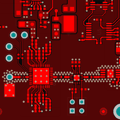
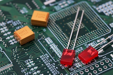
Modern PCB Design & Layout
We have experience designing PCBs for high speed digital systems, backplanes and daughterboards, optical systems, wireless/IoT products, power electronics, mmWave systems, and much more. We start with your schematic and BOM or your ECAD files, and we provide you with a finished PCB layout along with all standard manufacturing documentation and assembly drawings.
During the PCB design process, we keep an eye towards the scalability of your design, as well as standard DFM rules and implementing requirements from your manufacturer. If you have not consulted with a manufacturer, we can help you find a producer that will meet your needs and help you scale. Our collaborative approach reflects best practices and helps you reach success.
- Click an image to learn more or get started today.
PCB Design Software Support


![]()
![]()
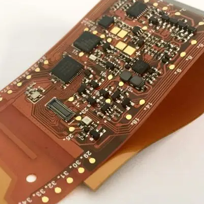
Turnkey Design and Manufacturing
In addition to PCB design and layout, we work with local and overseas manufacturing partners to get your board produced at your required volume. Instead of applying a large markup for these services, we bill hourly and pass the savings on to you.
- Quality and compliance - We only work with ISO-9001, AS9100, NADCAP, and ITAR/JCP certified manufacturing partners.
- Full design review and BOM cleaning - Each design is inspected for reliability and obsolescence.
- Consultation and quotes - We shop your design to our partners to get you the best price and lead time.
- Component sourcing - We help you navigate the electronics supply chain and produce at volume.
- Transparent pricing - We don't apply a markup to orders, we bill at a fixed rate for managed manufacturing.

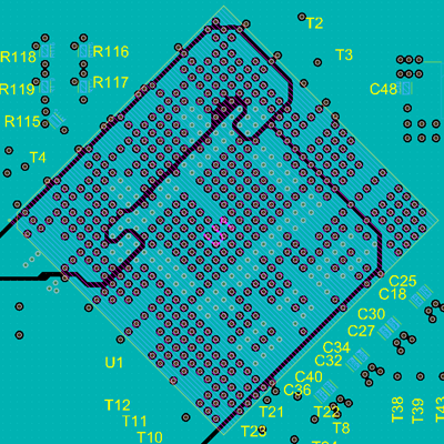
Design Verification: Power Integity, Signal Integrity, and EMI/EMC
Signal integrity and power integrity problems are the bane of many PCB designers, and some EMC failures originate as signal or power integrity problems. Power and signal integrity problems at the PCB layout level can cripple a new system, and they can be difficult to locate and solve.
Our extensive experience in PCB design and analysis makes us a natural choice for consulting on signal integrity, power integrity, and EMI issues in new, complex PCB designs. We're one of the few PCB design bureaus that runs all its own signal integrity simulations and analyses.
- Learn more about which analysis techniques you should use from our simulation and analysis cheat sheet.

Our PCB Design Workflow
At Northwest Engineering Solutions LLC, we follow a structured PCB design process to deliver high-quality, manufacturable PCB designs tailored to your exact specifications. Our expert PCB designers use industry-leading tools and best practices to ensure efficient, cost-effective solutions for various industries, including military PCBs, aerospace, robotics, automotive, and industrial electronics.
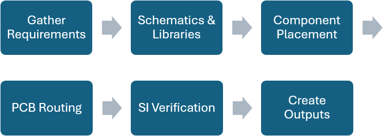
1. Project Initiation & Requirement Analysis
We begin with a detailed PCB design consultation to define your project’s technical specifications, functionality, and constraints. This includes reviewing schematics, mechanical design constraints, compliance requirements, and manufacturing preferences to ensure your PCB is optimized for both performance and production.2. Schematic Capture & PCB Library Creation
Using industry-standard schematic capture software, we translate your circuit design into a well-organized electronic schematic diagram that ensures logical connectivity and compliance with electrical design rules (ERC). Our team also develops and verifies PCB footprints, symbols, and 3D models, ensuring consistency and adherence to industry standards like IPC-7351.3. Optimized PCB Layout & Component Placement
Our PCB layout engineers strategically place components to optimize signal integrity, power distribution, thermal performance, and manufacturability. We ensure proper trace routing, impedance control, and mechanical compatibility to enhance performance and reduce electromagnetic interference (EMI) risks.4. PCB Routing & Signal Integrity Validation
High-speed signals, RF circuits, differential pairs, and the power delivery network (PDN) are carefully routed to minimize noise and interference. We apply advanced PCB routing techniques, including controlled impedance routing, layer stack-up optimization, and electromagnetic compatibility (EMC) analysis, to enhance reliability and efficiency.5. Design Verification & DFM/DFA Analysis
Before finalizing the PCB design, we perform Design for Manufacturability (DFM) and Design for Assembly (DFA) analysis to prevent costly design iterations. This step includes electrical rule checks (ERC), signal integrity simulations, thermal analysis, and compliance verification to ensure your design is optimized for mass production and testing.6. Fabrication & Assembly Documentation
We generate a complete PCB manufacturing package, including Gerber files, ODB++, drill files, a bill of materials (BOM), assembly drawings, and pick-and-place data. This ensures a seamless transition from PCB design to fabrication and assembly, reducing lead times and ensuring production efficiency.
PCB Design Tool Support
Altium Designer PCB Services
Altium Designer is the world's most popular PCB design software platform, offering a range of capabilities for advanced PCB designs and multidisciplinary engineering collaboration.
- Schematic Capture & Library Management – Creation and validation of schematic symbols, PCB footprints, and 3D models.
- Multi-Layer PCB Layout – High-speed signal routing, impedance control, and design optimization for manufacturability.
- HDI/UHDI PCB Design – Ultra-high density PCB design and IC substrate design with high layer counts.
- Altium 365 Collaboration – Seamless integration with Altium 365 for real-time collaboration, PCB design reviews, and supply chain insights.
- Manufacturing Outputs – Generation of Gerber files, ODB++, BOMs, and assembly documentation for streamlined production.
Xpedition PCB Design Services
Xpedition remains the preferred design platform among military and aerospace OEMs, enabling constraint-driven design for a broad range of electronic products.
- High-Density PCB Layout – Advanced routing for high-speed, RF, and mixed-signal designs, ensuring signal integrity and EMI mitigation.
- Constraint-Driven Design – Implementation of electrical, mechanical, and manufacturing constraints for first-pass success.
- 3D Mechanical Integration – ECAD-MCAD collaboration with native 3D visualization and STEP file integration.
- Enterprise-Level Workflow Support – Collaboration with PLM systems and automated design validation for efficient project execution.

Cadence OrCAD & Allegro PCB Design
Cadence supports complex PCB layouts with high-speed digital interfaces, high density component placement, high-reliability assemblies, and much more.
- OrCAD Schematic Capture & Constraint Management – Precise schematic design with intelligent constraint-driven layout.
- Allegro High-Speed PCB Layout – Expertise in DDR, PCIe, RF, and other high-speed digital interfaces.
- PCB Miniaturization & HDI Design – Layout optimization for fine-pitch components, rigid-flex PCB, and high-density interconnect PCBs.
- Comprehensive Manufacturing Support – Generation of industry-standard fabrication and assembly files, including IPC compliance verification.

Signal Integrity Verification with Simbeor
Fast analysis and full 3D electromagnetic simulation of PCB interconnects for standardized interfaces, such as PCIe, USB, DDR, and Ethernet.
- Impedance Control & Transmission Line Optimization – Accurate modeling and validation of PCB trace impedance to minimize signal distortion.
- Loss and Dispersion Analysis – Characterization of conductor and dielectric losses to enhance signal quality in high-speed interconnects.
- Crosstalk & Reflection Mitigation – Analysis and reduction of unwanted noise and signal integrity issues in dense PCB layouts.
- Material & PCB Stackup Optimization – Selection of optimal PCB materials and layer configurations to meet high-speed design requirements.

Related Resources
What Goes Into a PCB Layout Time Estimation?
By ZM Peterson • May 15, 2021Learn more about the factors affecting PCB layout time estimation and what you can expect when you engage with a design firm.

Your PCB Layout Review Checklist Before Manufacturing
By ZM Peterson • Nov 18, 2020Before you send your PCB out for manufacturing, run through a PCB layout review checklist to ensure manufacturability and conformance to design requirements.
Getting Started
Our goal is to streamline the innovation process for advanced electronics and help clients scale to volume production.- Contact us for a consultation and quote.
- Send us all available documentation on your design, including schematics and engineering BOMs. If you haven't created your schematics or they need updating, let us know and we'll work with you to make them perfect.
- We'll send you completed flat or hierarchical schematics, PCB layout, any required embedded software, fabricator documentation, Gerbers, assembly drawings, and manufacturing BOMs.
- Throughout the design process, we'll collaborate with you on any required design changes and provide suggestions to improve your new product.
Why Work With NWES?
- Broad expertise - We're a digitally-driven remote-first organization with diverse talent and experience. We know your technology because we've used it and built it.
- Manufacturing partners - We work with local and overseas CMs and EMS providers that are ISO-9001, AS9100, ISO-13485, IPC-A-610, NADCAP, and/or ITAR/JCP certified. We help you find the best option to produce prototypes and scale to volume production.
- Supply chain management - We take a proactive approach on projects to ensure your design can be produced at the required volume. We'll manage procurement from major distributors or brokers throughout your project.

Need a hand with a current or future PCB design project? Find out the difference our experts can make.
Contact us today for more information.
Our Clients and Partners


