
PCB Material Selection Guide
By ZM Peterson • Jan 22, 2025This guide covers material properties, application-specific selection, and key considerations for high-voltage, RF, high-speed digital, and HDI PCBs.
All electronic assemblies are designed through a specific workflow that ensures your device will be functional and manufacturable at scale. The PCB design process follows a logical order and is implemented in specialized CAD software. The goal is to generate a set of files that are used to fabricate and assemble your PCBA. If you've taken time to gather all functional and performance requirements for your new product, and you need to design a high-quality PCBA for your device, then you're ready to move through the PCB design process.

The schematic capture phase of the PCB design process involves the creation of electrical schematics and drawings that show how components are interconnected. Spice simulations may also be performed on critical circuits during this phase. Electronic schematics show connections between components and sub-assemblies that accurately capture the functionality of your device. Your block diagram and functional requirements are used as guiding documents during this stage of the PCB design process.
During schematic capture, the bill of materials (BOM) should be scrubbed and finalized based on the functional needs of your product. BOM cleaning is an important part of the PCB design process, especially considering today's volatile supply chain environment. The best PCB design services firms know that your PCBA and its components need to be manufacturable and sourcable, otherwise your new product might never be produced at the desired volume.

Before laying out the PCB, the layer stack should be planned by selecting materials, signal layers, plane layer pairs, and assigning each to different players in the circuit board layer stack. Once the PCB stackup is designed, it should be submitted to a fabrication house to ensure it can be manufactured as requested. It is often the case that a stack up will need to be modified before production. This will affect design aspects like impedance control, the ability to suppress EMI or propagation losses, and costs to an extent. Advanced electronics rely on a properly designed PCB layer stackup to ensure an electronic product will function as intended.

After the schematics are captured, reviewed, and approved, and after the layer stack is defined, component models are imported into a PCB layout for placement and routing. After defining the board size based on mechanical requirements, critical components are placed in the PCB layout with the goal of ensuring external and internal connectivity, as well as solvability during routing. The right component placement choices will help make routing easy while also preventing SI/PI/EMI problems.
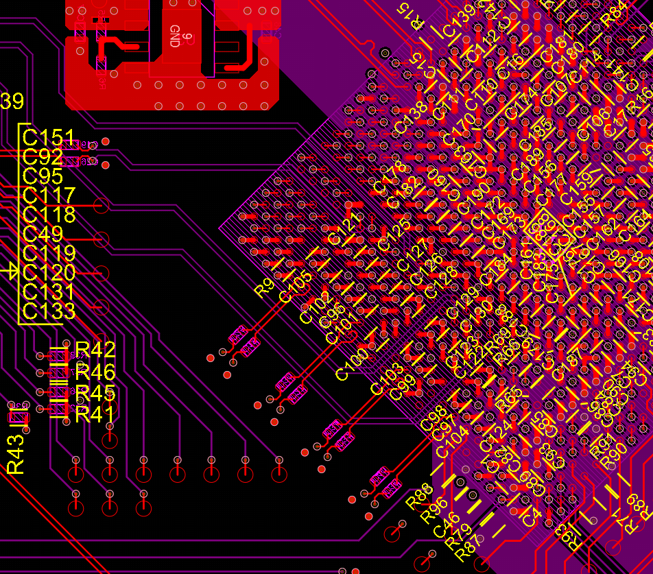
During the routing phase, traces, rails, transmission lines, and other printed circuit elements are placed around the board to complete the required electrical connections in the PCB layout. The routing phase must be done carefully to ensure your device has the required level of signal integrity, power integrity, and EMI/EMC compliance.
If the previous phases are completed properly, PCB routing will be much easier and less rework will be needed. In high speed PCBs and RF PCBs, transmission lines need to be carefully designed by accounting for losses and dispersion along signal routes, something which can be challenging at very high frequencies.
Advanced products require some level of verification after the PCB layout is complete. This is performed using specialized electromagnetic simulation applications. These applications can be used to identify signal integrity, power integrity, and EMI problems, all of which could cause EMC failure or performance failure during operation. Some of the important simulations that should be performed for evaluation include:

Once the PCB layout is finalized, a final design review should be performed to ensure all functional, mechanical, and performance requirements are met. It is actually advisable that design reviews be performed at each stage in the PCB design process. Usually, design reviews are performed at each the following stages:

Repeated PCB design reviews help ensure that any mistakes are caught early and that functional requirements for the product are satisfied. The final design review also involves performing DFM checks to ensure manufacturability, high-yield assembly, and reliability once the device is deployed in the field. Other aspects like design for testing can be checked during this stage, especially if the board is being developed as a prototype.
After the design is completed and approved, it is time to generate PCB manufacturing files. PCB manufacturers do not often use your native ECAD files to fabricate and assemble your pcb. Inside they use a specific set of files to create tooling and program automated processing equipment.
The main set of deliverables PCB fabrication and assembly houses need to produce a PCBA include:

Once these files are generated, the design can be sent into your manufacturer for quote and DFM review. Depending on the acceptance and inspection standards required in the product (IPC-A-600 or IPC 601x Class 2/3/3A products), the manufacturer may send change requirements as part of a DFM analysis report. Skilled designers know how to design to these standards, avoid change requirements, and get through a DFM review quickly.
If the BOM was cleaned during the schematic capture stage, then any obsolete, end of life, or out of stock components would be identified early, and critical components could be ordered before the design begins. Due to periodic shortages since early 2020, it is now best practice to source the critical components early, rather than waiting until the design is moved into manufacturing.

The PCB design process is one of data generation as part of a comprehensive product development process. PCB designers don't just work with other electronics engineers, they also work with mechanical designers to ensure form, fit, and function in a final product. They also have to work alongside application developers who will write firmware or software that controls the product and creates a meaningful user experience. By the end of the PCB design process, a wealth of design and manufacturing data will have been generated by an entire team of designers and engineers.
| Category | Data Type |
|---|---|
| ECAD | • Block diagrams and flowcharts • Electrical schematics • PCB layout for each board • Simulation models and results • CAD data for components (symbols, footprints, etc.) |
| MCAD | • STEP files (enclosures, assembly model, etc.) • STL files (if applicable) |
| Firmware/software | • Flowcharts and functional requirements that are needed to build and debug an application • All source code for the application • Any compiled HEX/BIN files for flashing to the device memory |
| Documentation | • All documentation needed to understand the internal workings of the product or its application • All documentation needed for users to clearly understand and use the product |
| Manufacturing | • Fabrication files (Gerbers, ODB++, IPC-2581, NC drill) • BOM with sourcing information • Assembly files (Pick-and-place) • Fabrication and assembly drawings • Test point information • Testing requirements |
This guide covers material properties, application-specific selection, and key considerations for high-voltage, RF, high-speed digital, and HDI PCBs.

PCB grounding is a fundamental system-level design consideration that will affect all aspects of noise and EMC in your PCB layout.

Before you send your PCB out for manufacturing, run through a PCB layout review checklist to ensure manufacturability and conformance to design requirements.


