
Guide to Signal Integrity Analysis in PCB Design
By ZM Peterson • Aug 31, 2020Signal integrity is a deep subject that relates to nearly every activity in high speed PCB design. Your stackup, layout, routing practices, use of impedance control, and many other design choices will influence signal integrity. Many designers rely on the bare minimum in their CAD tools for signal integrity analysis in PCB design, which puts their clients at risk of design failure.
If you want to do signal integrity analysis in PCB design correctly, you need the right set of mathematical tools and some basic simulation tools to help you along. Unfortunately, there is no single design task that will fix every signal integrity problem, and there is no single tool that will identify every signal integrity problem. In this guide, we’ll briefly cover the following topics:
- Math Tools for Signal Integrity Analysis in PCB Design
- What Signal Integrity Metrics to Analyze and Simulate
- PCB Layout Choices to Ensure Signal Integrity
One area I would love to cover but simply don’t have enough room to do so fully is test and measurement, specifically around signal integrity and power integrity. Note that the two areas are related, and studious designers should take note that failure in power integrity can cause failure in signal integrity. For now, let’s focus on the signal integrity aspect and some important metrics to calculate during and after the design phase.
Math Tools for Signal Integrity Analysis in PCB Design
Signal integrity is basically a ton of math on the front-end, where the design is still being planned and certain high speed/high frequency structures in your PCB are being designed. You’ll need a few different tools for running basic calculations from data (either measured or simulated) as you design different structures and determine their signal integrity metrics.
As such, you’ll need some basic tools to help you wrangle data, like MS Excel or a more powerful set of programs like Mathematica, MATLAB, or a scripting language like Python. Scripting tools can be a bit wonky if you’ve never worked with them for complex math problems. I prefer Mathematica since it’s still a scripting language, but it automates a lot of the math through its symbolic manipulation features. This way, I don’t need to write out every mathematical function in Python or keep adding new libraries for each calculation.
MATLAB is a great tool and many of the standard calculations you’d need to perform are built into MATLAB. This includes calculations that are specific to network analysis, which is an indispensable part of signal integrity analysis in PCB design. Some of these tasks include:
- Circuit design and simulation tools. SPICE simulators are the cornerstone of modern circuit design and evaluation. They basically automate a complex matrix algebra problem and return electrical data at any point in your circuit.
- Fourier and Laplace analysis. These are applicable in circuit design, transmission line design, and any other area of signal integrity analysis in PCB design involving conversions between time-domain data and frequency-domain data.
- S-parameter manipulations. I’ve always thought S-parameters were a bit overgeneralized, but they have conceptually satisfying meanings in specific situations. You’ll often need to convert between different parameters.
- Signal processing tasks. Fourier/Laplace analysis is probably the most common task, but there are many other tasks that you might need to perform as part of wrangling waveform data from measurements or simulations. Convolution, statistical analysis, and regression are a few examples.
- Optimization tools. MS Excel includes three basic optimization algorithms as part of the Solver package, which you can use for signal integrity analysis in PCB design. These are an evolutionary algorithm with constraint handling, generalized reduced gradient (GRG Nonlinear), and simplex algorithms. These are easy to access, configure, and execute when you have a large set of interrelated data. More advanced optimization problems (multi-objective, numerical, discrete, etc.) require specialized tools or scripting.
- 3D EM field solvers. Advanced design tools will contain field solvers for automating certain signal integrity tasks. When you’re designing unique design structures or you need to visualize EMI emissions/reception in your board, a field solver is by far the best tool you can use.
Having the right set of analysis tools is half the battle. There are certain signal metrics you should simulate to the best of your abilities when examining signal integrity. Any signal integrity analysis metric in PCB design is related back to the physical layout or circuit design in some way. Therefore, you’ll need to use interpolated field solver results or analytical formulas to derive important signal integrity metrics in your PCB. While we can’t touch on every single metric in a single guide, we can help you determine where to look for this information. Take a look at the next section for a brief summary of some signal integrity simulation tasks and what you want to quantify as part of signal integrity analysis in PCB design.
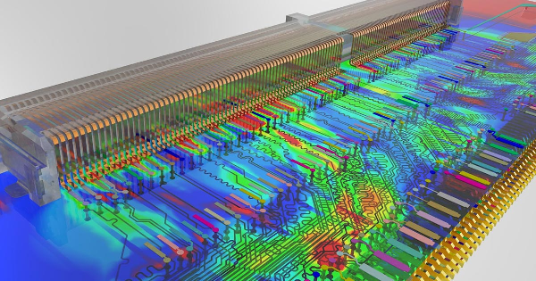
A 3D field solver can help you visualize important signal integrity metrics as you analyze your board.
What Signal Integrity Metrics to Analyze and Simulate
Once you’ve got the tools you need to perform some important mathematical calculations and other tools to examine your PCB layout, you can figure out what specific metrics you need to analyze within your PCB. Most signal integrity problems are related to the following three areas:
- Transmission line design
- PCB stackup design and laminate selection
- Routing in your PCB layout
These areas should be starting points for designing your high speed/high frequency board and for signal integrity analysis in PCB design. If you can extract important insights in these areas, your board is more likely to work correctly the first time.
Impedance and S-parameters in Transmission Lines
These two points are related and are a cornerstone of signal integrity for high speed and high frequency designs. High speed/high frequency signals require impedance control as long as an interconnect is electrically long. As such, the designer needs to carefully design transmission lines to have the desired impedance to prevent reflections and subsequent resonances.
S-parameters are one way to nicely summarize reflection at one end of an interconnect, as well as losses as a signal travels down an interconnect. The former is embodied in return loss (S11), which is related to any impedance mismatch between the transmission line and the load. The latter is quantified as insertion loss, which accounts for all losses as an injected signal travels from the source to the load. These two metrics are normally the metrics that are used to determine whether a transmission line will conform to a given signaling standard. You can calculate these values by hand, or you can use some software to calculate these values from your PCB layout.
- Learn more about impedance matching used in high speed signaling standards.
- Learn more about dispersion and losses in your transmission lines.
- Learn more about S-parameters in your transmission lines.
Eye diagrams are another important point to simulate in signal integrity in PCB design. Some of the best analysis tools will allow you to simulate an eye diagram (e.g., Simbeor) from a pseudorandom bit stream or from randomly distributed jitter, as defined in a component datasheet. This simulation is quite useful as it provides some important metrics in high speed signaling standards that can be directly compared with measurements.

Eye diagram for a failed DDR channel showing excessive overshoot and undershoot.
PCB Stackup Design and Laminate Selection
Your PCB stackup plays an important role in providing isolation. Your stackup determines the trace width you need to select for impedance, as well as the level of isolation in your PCB. Your layer stackup will also determine the amount of routing space available in your board. When analyzing signal integrity, an important point is to calculate the parasitics in your board, which are partially related to stackup design. In particular, the parasitics should be as low as possible while still providing controlled impedance and isolation between signal layers. In addition, place power planes adjacent to ground layers in order to provide the required level of interplane capacitance in the board and to ensure low PDN ripple in your PCB.
The laminate you select will have a specific dielectric constant, which defines the level of losses and dispersion in your PCB layout. Most signal integrity engineers say you should opt for a low Dk laminate, but a high Dk laminate also has some merits in terms of power integrity and low loss tangent. Be sure to include losses and dispersion in your transmission line impedance and S-parameter calculations when simulating your board.
- Learn more about PCB layer stackup design to ensure signal integrity.
- Learn more about the causes of ripple voltage due to transients on your PDN.
Another important point to remember in stackup design is that your PDN normally includes decoupling/bypass capacitors to ensure low impedance throughout the required signal bandwidth. These capacitors have their own parasitics, which then influence the appearance of resonances in the PDN impedance spectrum. Power integrity is intimately related to your PCB stackup and signal integrity in your board.

Decoupling capacitors include their own parasitics that produce self-resonances, which need to be included in signal integrity simulations.
Routing and Signal Integrity
How you route your signals will determine how much crosstalk they induce in each other, as well as the number of signals you can fit into each layer. Whether you’re using single-ended or differential signals, crosstalk will be influenced by parasitics between interconnects, which will allow noise to couple between signal lines. In dense boards, you need to balance placing small spacing between traces with allowable crosstalk. Placing traces closer together increases parasitic mutual capacitance between traces and it increases the magnetic field strength seen at a trace, both of which create stronger crosstalk.
In parallel nets and differential pairs, length matching is needed to prevent skew between signals and to ensure common-mode noise rejection at receiver components, respectively. If you’re working with these types of nets, you should perform a simple skew calculation to ensure you’ve determined the allowed length mismatch. Some CAD tools will do this for you; you only need to look up the allowed timing skew from datasheets. Less advanced CAD tools will only accept a length mismatch value, but the critical parameter is the time mismatch, which depends on the dielectric constant of the substrate.

These length matching structures help ensure signals have low skew.
Eye diagrams are another important point to simulate in signal integrity in PCB design. Some of the best analysis tools will allow you to simulate an eye diagram (e.g., Simbeor) from a pseudorandom bit stream or from randomly distributed jitter, as defined in a component datasheet. This simulation is quite useful as it provides some important metrics in high speed signaling standards that can be directly compared with measurements.
Note that your board can be designed to receive a perfect grade in every signal integrity metric, but a poorly design stackup and routing can still be prone to receiving external EMI. Thanks to electromagnetic reciprocity, it may also be a strong emitter of EMI, which can cause it to fail EMC tests. A full-wave 3D field solver (either FDTD or FDFD) will let you visualize the near-field or far-field radiation emitted from your board as it operates. This helps you identify specific areas of the board from which EMI originates, and you can get a clue as to whether you’re likely to fail an EMC test. Simple choices regarding stackup design and routing can often solve most EMI problems and help you pass EMC.
At NWES, we’ve designed simple 2-layer and complex HDI PCBs for digital and analog systems. We’re experts in signal integrity analysis in PCB design and we can help ensure your next PCB operates as you intend. We're here to help electronics companies design modern PCBs and create cutting-edge technology. We've also partnered directly with EDA companies and advanced PCB manufacturers, and we'll make sure your next layout is fully manufacturable at scale. Contact NWES for a consultation.
Ready to start your next design project?
Our Clients and Partners


