
Conducted and Radiated EMI in Your PCB Layout
By ZM Peterson • Nov 1, 2019If you want your new product to pass FCC and CISPR EMC tests, then you need to control conducted and radiated EMI from your board. The conducted EMI portion is defined in terms of the amount of noise that is sent through the AC return line between 150 kHz and 30 MHz.
Meanwhile, the radiated EMI portion is defined in terms of the radiation emitted from a board at some specific distance (10 m from the board). Conducted EMI comes in multiple forms, primarily originating from various noise sources in one component and propagating downstream to another component. Controlling radiated EMI from interconnects, components, and plane layers requires controlling the electromagnetic field. When considering the wealth of parasitics in your layout, you need to optimize the geometry of your conductors and placement of components. This may sound esoteric, but it essentially means you are examining two aspects of your PCB design:
- Bandwidth of signals and components (conducted EMI)
- PCB stackup and routing topology (radiated EMI)
PCBs are complicated systems, and these two aspects of EMC are intimately related. Let's take a look at both aspects of EMI and examine how you can make some simple design decisions that address both aspects.
Conducted and Radiated EMI Sources
Conducted and radiated EMI are interrelated; one source of EMI in one portion of the board can produce the other source of EMI in another portion of the board, leading to complicated coupling. For conducted EMI, we can point to the following noise sources:
- Amplified noise. Noise (e.g., Johnson-Nyquist noise, 1/f noise, or any other induced/coupled noise) present on the input in an amplifier run near saturation can be amplified while the desired signal is compressed. This decreases the signal-to-noise ratio.
- Spurious harmonics. These frequencies can arise from a nonlinear or nearly-nonlinear component. This generates harmonics of some fundamental signal or intermodulation products. This is then seen as distortion on the output from the component in question.
- Switching noise. This is a particular problem in switching regulators, which pass noise peaks corresponding to the internal PWM signal onto the regulator output. This is normally filtered with an output capacitor.
- Power bus ringing. This results from insufficient decoupling on the power bus. This is also a source of radiated EMI, as the strong burst of current and resulting ripple on the power bus creates an electromagnetic pulse. In terms of conducted EMI, this can pass some ripple to the output from an IC as it interferes with the supply voltage seen by transistors. This also produces timing jitter/phase noise.
- Unideal clocks. There is no ideal clock pulse; every clock pulse carries some spurious frequency content that can produce conducted and radiated EMI. Using spread spectrum clocking is one way to reduce EMI in digital systems with real clocks.
- Any other induced/coupled signal that originates from radiated EMI.
As signals travel on your interconnects, they emit some electromagnetic radiation into the board and the surrounding environment. In addition to spurious clock frequencies and power bus ringing, we have the following sources of radiated EMI:
- Cavity resonances in your board. Your board will contain a number of cavities, each of which has some group of electromagnetic resonances. An electromagnetic wave emitted from anywhere on your board can excite a resonance on your board. Cavities are formed by the fiber weave in your substrate, and the arrangement of planes and traces in your stackup.
- Standing waves on unterminated transmission lines. This occurs when particular frequencies reflect between a driver and a source on a mismatched transmission line. This is easy to understand with analog signals, but it also occurs at certain harmonics in a digital signal. In this case, the transmission line acts like a strong radiating antenna.
- Any source of conducted EMI that induces a signal in a radiating element or cavity.
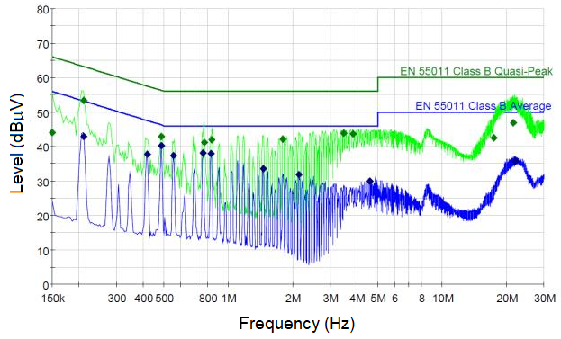
Example radiated EMI peaks measured during an EN 55011 Class B EMC test.
Schematic simulation tools (e.g., SPICE and other pre-layout simulation tools) can help you simulate many aspects of conducted EMI, but this will only take you so far as pre-layout simulation tools cannot account for parasitics. You'll need to use a 3D post-layout simulation application to identify board resonances and determine how radiated EMI propagates away from the board.
Suppressing Conducted and Radiated EMI
As much as we would like, we cannot address every conducted and radiated EMI problem in a single article. Each of these points is complicated in its own right. However, we bring up some general points to consider when addressing conducted and radiated EMI.
Conducted EMI
As conducted EMI results from passing noise between components in a board through conductors, you'll need to use filtration at certain points to suppress specific noise sources. As long as you can identify the particular frequencies you need to suppress, then you can determine the type and level of filtration you need.
Continuous, uncorrelated noise sources (Johnson-Nyquist noise, 1/f noise, shot noise) are more difficult to address as they cannot be removed from a particular analog signal with filtration. You'll have to take other steps to reduce the noise floor in particular components. In addition, if there is broadband conducted EMI on a signal you are gathering from the surrounding environment (e.g., from a sensor or antenna), then you need to isolate the conductor receiving the noise. You can also take some basic signal processing steps when converting the signal to digital data.
Radiated EMI
If you look at the list above, you'll see that resonances on a mismatched transmission line produce strong EMI with high-Q resonance. Therefore, you should always terminate transmission lines to prevent reflections. Second, power bus ringing causes a strong pulse of radiation as current is drawn into your PDN. The radiated power is proportional to the transient power in the PDN (i.e., the transient ripple voltage multiplied by the burst of current drawn into the PDN). You can’t reduce the current, but you can minimize the transient voltage ripple by minimizing the PDN impedance.
Although board resonances can have a complicated structure, you can easily suppress board resonances (both from the fiber weave and the arrangement of conductors on the board) by placing grounded, stitched via fences around high power RF circuits and around the perimeter of your board. The via spacing will create an image plane (read more on this here) with respect to the radiating conductor and resonator, which will reduce the strength of the electromagnetic field emitted from the board. The appropriate via spacing is:

You can get an idea of the lowest order resonance by looking at the spacing between plane layers. The distance between plane layers is roughly equal to a half wavelength inside the dielectric, which can be converted to its corresponding frequency.

Lining up a grounded via fence along the edge of your board, similar to these stitching vias along a trace, will create a strong image plane that helps suppress radiated EMI from PCB cavity emissions.
When you consider the different radiated EMI mechanisms, you’ll need to select the right stackup in order to control electric fields in your board. Overcoming resonances in the fiber weave cavities requires using FR4 or other laminate with much tighter weave pattern, or using a substrate that is completely solid. The right stackup design for ensuring EMC/EMI tests are passed is its own specialized topic, which we’ll look at in an upcoming article.
Diagnosing conducted and radiated EMI problems in your board can be difficult, but working with the right design and research firm can help you solve these problems and determine the right PCB design choices to help you pass EMC tests. If you’re looking for a knowledgable firm that offers cutting-edge PCB design services and thought leadership marketing services for electronics companies, contact NWES for a consultation.
Ready to start your next design project?
Our Clients and Partners


