
Causes of Ripple Voltage: Power Supply Noise and Transients in Your PDN
By ZM Peterson • Oct 29, 2019If you’re examining the stability of your power supply voltage with an oscilloscope, you’ll always find some noise in the time and frequency domains. As part of PCB design, your goal is to identify various noise sources and take steps to reduce them.
Simple steps like filtration and decoupling capacitors are appropriate for particular noise sources, but they will not provide sufficient decoupling when working with very fast digital signals (less than ~1 ns rise time, according to Rick Hartley). As part of PCB design, particularly signal integrity and power integrity analysis, understanding how different noise sources appear in the frequency and time domains helps you identify your noise sources. Here’s how ripple voltage sources and other noise sources create power integrity problems in your board and how to spot ripple voltage in your PDN.
Causes of Ripple Voltage and Power Supply Noise
Intrinsic noise from your power supply and on the power rails in your PCB comes in four forms:
- Random noise in the frequency domain. This noise appears as thermal noise (i.e., Johnson-Nyquist noise) throughout the frequency domain. This white noise (i.e., spanning throughout the frequency spectrum) is Gaussian distributed (i.e., changes in the magnitude in time follow a Gaussian process).
- Switching noise. This appears at specific frequencies on the output from a switching regulator (buck-boost converter, flyback/forward converter, VRM, etc.). This noise arises from the PWM signal used to switch one or more FET drivers in the converter.
- Ripple from AC-DC conversion. This is seen on the output from unregulated, unfiltered power supplies that convert an AC input to a DC output. This is leftover from the full-wave rectifier used for power conversion.
- Transient ringing. This type of oscillation looks like ripple from power conversion, but it is fundamentally different. This arises from the parasitic capacitance and inductance in the PDN. As an IC switches states or output levels, it draws a burst of current that produces a transient oscillation, which is sometimes called a ripple voltage. This transient response can appear on the power rails even if the supply voltage is regulated.
As a designer, your job is to anticipate when these different noise sources will be prominent and take steps to remove or suppress each noise source.
There is a fifth source of noise that we haven’t discussed, although it is related to PWM switching noise in a switching regulator as mentioned above. The output from a switching regulator will contain switching noise at ~kHz frequencies (conducted EMI), which can easily induce a current in a downstream circuit. Although this conducted EMI is normally removed with filtration, a switching regulator can induce noise in a downstream circuit as radiated EMI. In regulators that supply significant current (~5 A or more), the parasitic inductance of downstream circuits is large enough (usually ~nH) that a significant voltage spike can be induced. This spike can be large enough to cause unintended switching, increasing bit error rates. At minimum, this will increase jitter/phase noise in a downstream IC.
Ripple Voltage: Power Rail Ringing or Smoothing Capacitor Ripple?
The primary difference between ripple from a smoothing capacitor and transient ringing is in the frequency at which the oscillation is observed. A rectifier bridge used for AC-DC conversion takes a 60 Hz or 50 Hz sinusoidal power source and converts it to its absolute value, which is then converted to a DC signal with a smoothing capacitor. The smoothing capacitor in the rectifier bridge discharges twice per cycle, so the output from the rectifier includes a ripple at double the frequency of the input AC signal. You can reduce the impact of this particular frequency with a bandstop filter. However, this still leaves the output unregulated, meaning the voltage seen by the load will vary if the load impedance changes.

Fig. 1: Ripple voltage from a rectifier bridge with a smoothing capacitor.
Normally, the output from an AC-DC converter, which can be regarded simply as an unregulated power supply, is then input into a regulator (usually a switching regulator). A regulator is designed to hold the output voltage constant against changes in the load on the output, which is common when dealing with nonlinear circuit elements (transistors, diodes, etc.). While holding the voltage constant, the device outputs some current up to some maximum value. The regulation is provided by a diode and switching a FET driver, which is driven with a PWM single. As a result, this suppresses ripple from a rectifier bridge, but it produces the switching noise mentioned above. Noise from a power regulator does not appear as a smooth low frequency oscillation. Instead, it appears as a high-Q peak in the frequency domain, usually at ~100 kHz frequencies.
Now contrast this with a transient ripple voltage. The transient ripple voltage appears at higher frequencies corresponding to the damped transient oscillation frequency in the PDN. This typically appears as an underdamped oscillation during a single switching event, although it could appear as a damped oscillation on the PDN. This can also appear as a forced oscillation, as shown in the signal trace below (Fig. 2).
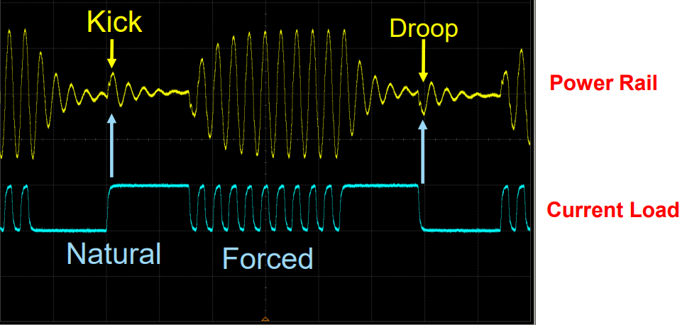
Fig. 2: Transient ripple voltage on a power rail as an IC switches. Image credit.
Fig. 3 below shows how a transient ripple voltage propagates through a system. During the schematic and PCB design phases, you’ll need to simulate the behavior of your PDN design with a post-layout tool in order to take account of parasitics. The goal is to ensure that the PDN impedance is below some target value, which will ensure the ripple voltage less than the noise margin in your ICs.

Fig. 3: Transient ripple voltage propagation through a PCB due to a switching IC. Image credit.
With ECL and other fast logic families, the best way to ensure proper decoupling is to use power and ground planes in the internal board layers in order to ensure the PDN impedance is sufficiently low. This arrangement, alongside some decoupling capacitors between the power and ground points in your board, will form a parallel arrangement of capacitors, which will provide sufficiently large capacitance to ensure decoupling. This is reduces the number of required decoupling capacitors in your PDN. Watch out for self-resonance frequencies of capacitive elements in your PDN as these are responsible for the peaks and valleys seen in the PDN impedance spectrum.
Diagnosing power and signal integrity problems in your board can be difficult, but working with the right design and research firm can help you solve these problems and determine the right PCB design choices to suppress ripple voltage on your PDN. If you’re looking for a knowledgable firm that offers cutting-edge PCB design services and thought leadership marketing services for electronics companies, contact NWES for a consultation.
Ready to start your next design project?
Our Clients and Partners


