
PCB Design Services
By Altium Designer Experts
Northwest Engineering Solutions provides PCB design and layout services delivered natively in Altium Designer®. We use Altium's rules-driven workflow to translate your requirements into enforceable constraints so your schematics, layout, libraries, and manufacturing outputs stay consistent as the design evolves.
Our Altium-centric process is built for rapid iteration without losing functionality. You get a clean project structure, verified libraries and footprints, review-ready outputs for stakeholders, and a manufacturing package that is organized and repeatable reducing rework, avoiding preventable respins, and accelerating the handoff to your CM.
- Learn more about our expertise in the PCB industry.
Altium Designer Capabilities
Altium is a global software company that provides PCB design tools and resources. The company's most popular product is Altium Designer, a software program that empowers engineers throughout the entire PCB design and layout process. The software combines electronic computer-aided design (ECAD) libraries, rules and constraints, bill of materials (BOM), supply chain management, engineering change order (ECO) processes, and other important tools in one comprehensive, easy-to-use program.
For customers, our Altium expertise shows up as better control of the details that cause schedule slips: library quality, constraint definition, rule coverage, and release packaging. We build projects so another engineer (or your manufacturer) can open the design and immediately understand what's required without reverse-engineering intent from ad-hoc notes.
With Altium 365, we can support secure review workflows and distributed collaboration when your team spans engineering, compliance, and manufacturing. The result is faster feedback loops and fewer late surprises between prototype and production.
- Hierarchical and multichannel schematic design
- CAD tools for component creation and PCB layout
- High-speed PCB design and signal integrity tools
- Library and component management in a single platform
- Instant PCB manufacturing deliverable generation
- Integrations with 3D EM, MCAD, Jira, and version control
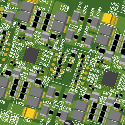
Key Features
The schematic editor in Altium Designer is your entry into a new design. Use the built-in CAD and simulation features to create and evaluate your design:
- Circuit design tools for building professional schematics
- Access to a massive component library with supplier links
- Integrated SPICE engine for circuit simulation and analysis

The PCB Editor in Altium Designer was built with CAD functionality in mind, giving a designer every tool they'll need to create professional layout documents and prepare for full-scale manufacturing:
- Highly accurate CAD tools for component placement and copper feature definition
- Create modular blocks to quickly build and reuse portions of a PCB layout
- Integrated field solver for impedance calculations in your PCB stackup
- Post-layout simulation toolset for advanced design and analysis tasks
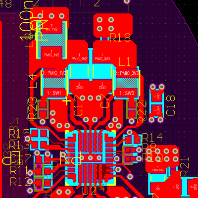
Altium's advanced routing features are built to handle everything from DC power systems to ultra-high-speed digital systems and high-frequency analog systems in a single program:
- Standard single-end and differential routing features that obey custom design rules
- Any angle routing, length tuning, pin swapping, and BGA fanout applied automatically
- Auto-interactive routing helps speed up routing in designs with high net count
- Easily route advanced interfaces like DDR4, PCIe, USB, HDMI, and much more
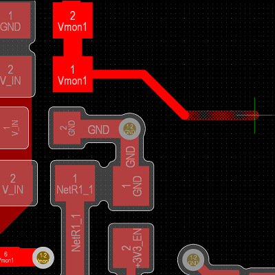
High speed design takes care and planning to ensure success. Altium Designer's toolset was built to help ensure every designer can conquer high speed layout and routing:
- Automatically enforce trace width and spacing during routing
- Easily enforce impedance results as design rules on specific nets
- Simulate crosstalk and reflection waveforms in your PCB layout
- Spot return path violations to prevent signal integrity problems and EMI
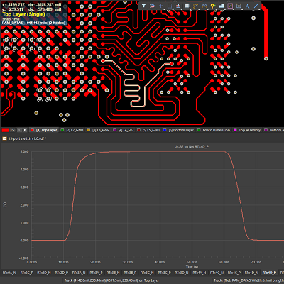
The design rules engine in Altium Designer is unique in that it checks a design as it's created and communicates with all other features in the Schematic Editor and PCB Editor.
- Catch errors early before they force a redesign
- Run DRCs on demand
- Quickly jump to errors in design documents
- Automatically generate reports to prove conformance

In addition to creating components with standard CAD tools, Altium Designer gives users access to the electronics supply chain with real-time sourcing and inventory data.
- Create high pin count schematic symbols and PCB footprint data
- Generate IPC-compliant PCB footprints and land patterns
- Easily create and modify libraries for your project
- Access real-time supply chain data directly from authorized distributors
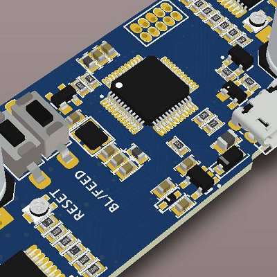
You shouldn't need an external program to prepare manufacturing files. Altium Designer will generate these for you with the OutJob file feature.
- Create fabrication files in standard Gerber file formats
- Create drill drawings, drill files, and pick-and-place files
- Generate any drawing you can imagine with Draftsman
- Compile sourcing data into your BOM and export data for assembly
- Apply settings to your manufacturing files automatically with templates
Enterprise Integrations
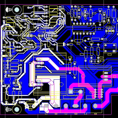
With a complete set of enterprise-level integrations available in Altium 365, we can deliver more advanced designs that require collaboration with MCAD software users, act on a dynamic electronics supply chain, perform critical validation steps in simulation, and reduce product lifecycle risk.




Our Work in Altium Designer
Mission-Critical Military Electronics
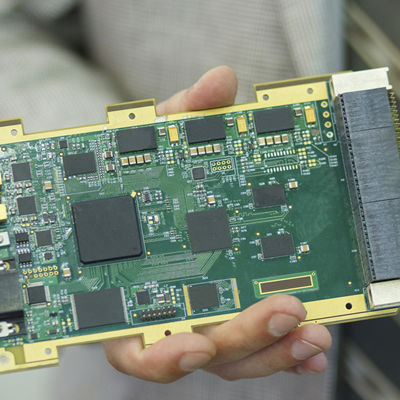
From terrestrial systems to space systems, defense and UAS programs are driven by SWaP constraints, ruggedization, and mission reliability. We build these designs to be rugged and scalable, with long lifecycles demanded in today's defense systems.
- SOSA/CMOSS-aligned VPX/OpenVPX embedded systems that enable seamless chassis level integration with modern defense platforms.
- SWaP-constrained avionics (including VITA 74/VNX & VITA 90/VNX+), flight-control, and communications for UAS and weapons systems, integrating IMU/GNSS, telemetry, and power management.
- Ruggedized mission payload electronics for manned and unmanned aircraft (EO/IR camera interface, gimbal control, onboard compute, and high-speed data links).
- Secure SATCOM systems and PNTR modules aligned with commercial spacecraft, military spacecraft, and defense modernization programs.
Industrial Systems & Automation
Industrial electronics are experiencing a revolution and a wave of new investment in production capacity as companies work to reshore production and modernize factories. Shorter supply chains and faster iteration cycles demand designs that are easier to build, test, and maintain at scale.
- Industrial control and I/O boards (PLC-adjacent modules, sensor hubs, actuator interfaces) designed for rugged connectors, isolation, and field reliability.
- Power conversion and power-entry electronics (DC-DC, protection, filtering, and distribution) for cabinets, machines, and factory-floor equipment.
- Condition-monitoring and instrumentation modules (precision sensing, data acquisition, and wired/wireless gateways) built for noisy environments and scalable deployment.
Medical Device Electronics
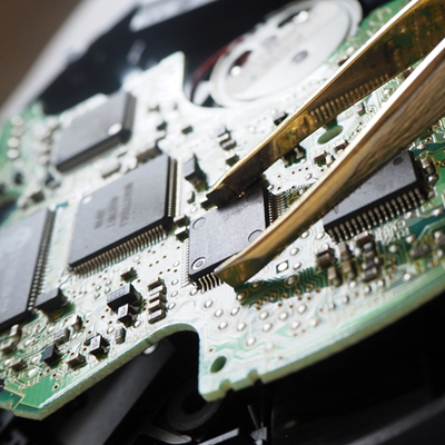
Medical device electronics demand disciplined design, traceability, and documentation to support regulatory review and long product lifecycles. We use Altium Designer to create PCB databases where constraints, libraries, and manufacturing outputs are explicit and reviewable.
- Patient-connected and patient-adjacent electronics with defined isolation and safety partitioning
- Diagnostic and monitoring systems combining precision analog front ends and embedded processing
- Implantable and wearable electronics focused on low power and compact form factors
- Medical power and interface boards designed with EMC and patient safety in mind
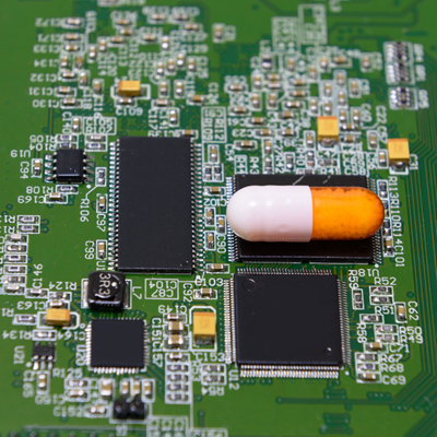
Edge AI, IoT, and Embedded Systems
Modern embedded products are being pulled in two directions at once: smaller form factors and higher local compute for AI inference. We build Altium projects that stay maintainable as complexity grows: clean hierarchy, reusable blocks, and constraint coverage that keeps mixed-signal behavior predictable through revisions.
- Battery-powered sensor nodes (BLE/Thread/Wi-Fi) with onboard sensing, power management, and compact antennas for small enclosures.
- Edge-AI vision modules combining an image sensor + compute + high-speed memory in a tight form factor for cameras, inspection, or robotics.
- Miniaturized wearables and portable instruments using dense mixed-signal front-ends and rigid-flex or space-constrained PCB layouts.
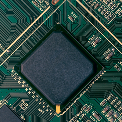
AI & Cloud Infrastructure at 224G+
AI infrastructure is pushing board-level links into ever-higher SerDes generations. In Altium Designer, we implement the constraint system, routing strategy, and documentation discipline needed to keep high-speed channels reviewable and reproducible, especially around vias, breakouts, and reference transitions.
- High-speed IO cards and modules (switch/retimer/PHY-centric designs) for data-center connectivity and scale-up/scale-out infrastructure.
- Compute- and accelerator-adjacent boards with dense connectors, high-speed memory interfaces, and tightly controlled high-current power delivery.
- High-speed backplane or mezzanine interconnect designs where connector selection, breakout geometry, and reference integrity dominate channel risk.
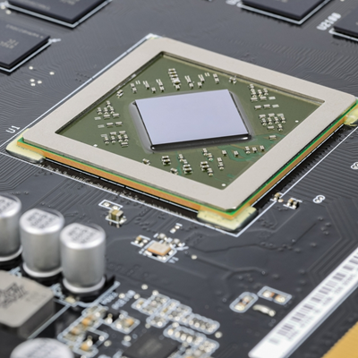
Our Process
Altium projects succeed when design intent is encoded into the database. Our process is built around making constraints explicit, keeping libraries trustworthy, and producing a release package that another engineer and your manufacturer can use without interpretation. As the design matures, we use a validation-minded workflow to reduce risk before prototypes, enforcing high-speed constraints, ensuring SI/PI/EMI, and performing in-house DFM analysis, ensuring the released manufacturing is scalable to volume production.
- Define requirements & constraints - Capture electrical, mechanical, safety, and compliance targets from the product specification and translate them into Altium rules, net classes, and design constraints.
- Libraries & schematic capture - Validate symbols/footprints and complete front-end circuit design and schematic capture with rules and classes implemented early.
- Layout with continuous verification - Perform placement, planes, routing, and DRC checks continuously while preserving constraint coverage; the completed layout is also checked in DFM and SI/PI/EMI tools.
- Release a manufacturing-ready package - Generate industry-standard fab/assembly outputs, drawings, and release artifacts aligned to the validated design intent for prototyping and volume builds.
Additional PCB Design Software Support


Take Your Design Into PCB Manufacturing
Manufacturing handoff is where many projects lose time. We use Altium's release and documentation utilities to produce a manufacturing package that is consistent, complete, and repeatable across spins:- PCB manufacturing outputs - Fab/assembly files (Gerbers, IPC-2581, ODB++) generated from a controlled release process.
- Supply chain visibility - BOM structure and sourcing context prepared for procurement and CM quoting workflows.
- Standardized documentation - High-quality drawings and notes organized so fabrication and assembly expectations are clear.
- Guiding the design to production - We provide additional technical guidance needed to get the design quoted, or work with our CM partners.
Why Work With NWES?
- Broad expertise - We're a digitally-driven remote-first organization with diverse talent and experience. We know your technology because we've used it and built it.
- Manufacturing partners - We work with local and overseas CMs and EMS providers that are ISO-9001, AS9100, ISO-13485, IPC-A-610, NADCAP, and/or ITAR/JCP certified. We help you find the best option to produce prototypes and scale to volume production.
- Supply chain management - We take a proactive approach on projects to ensure your design can be produced at the required volume. We'll manage procurement from major distributors or brokers throughout your project.

Need a hand with a current or future PCB design project? Find out the difference our experts can make.
Contact us today for more information.
Our Clients and Partners



















