
PCB Design Services
By Cadence Experts
Northwest Engineering Solutions provides PCB design and layout services delivered natively in Cadence OrCAD® Capture and Allegro® PCB Editor. We use Capture-based design intent, CIS-driven part data, and defined constraints to translate your requirements into designs that align with your performance demands and manufacturing capabilities.
Using OrCAD/Allegro's enterprise-level design tools, we focus on reaching performance targets on the first build while avoid preventing respins at all stages of product development. This ensures schematic intent, layout execution, and manufacturing deliverables remain aligned through revision cycles and ECOs.
- Learn more about our expertise in the PCB industry.
Cadence PCB Capabilities
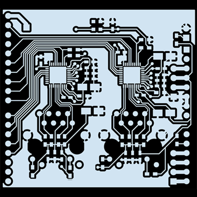
Cadence is a major EDA vendor whose OrCAD® and Allegro® platforms cover the full PCB flow, from front-end schematic capture through constraint-driven PCB layout and manufacturing release. OrCAD Capture supports scalable schematic development and part-property management, while Allegro PCB Editor provides the performance and constraint infrastructure used in complex designs.
We leverage the entire Cadence OrCAD/Allegro PCB design feature set to ensure complex designs are auditable and scalable into volume production.
- Hierarchical and constraint-aware schematic design in OrCAD Capture
- OrCAD Capture CIS provides system-level design capabilities and library governance
- Allegro PCB Editor for high-density placement, advanced routing, and DFM
- Constraint Manager gives control over electrical, physical, and manufacturing rules
- Manufacturing deliverable generation (Gerber/ODB++/IPC-2581, NC drill, drawings)
- Integrations with MCAD, simulation, PLM, and enterprise change control
Key Features
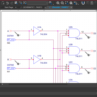
OrCAD Capture is where design intent begins, involving definitions of correct net structure, clear power domains, and property discipline that supports later constraint enforcement and manufacturing deliverable generation:
- Hierarchical/multi-sheet organization with reusable circuit blocks
- Capture CIS properties for part selection, alternates, and lifecycle fields
- PSpice-ready schematics for pre-layout validation of critical circuits
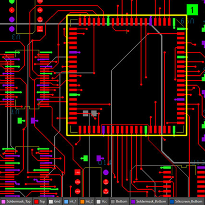
Allegro PCB Editor is designed for production layouts with constraint-aware placement and routing that keeps you compliant with DFM/DFA constraints. We use placement and routing discipline to avoid layout surprises that show up during DFM or bring-up:
- Accurate placement and copper-shape definition for complex assemblies
- Constraint Manager ensures routing and placement rules are enforced during layout
- Post-layout checks aligned fabrication and assembly constraints
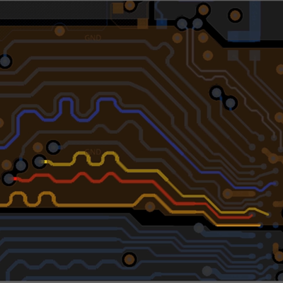
Allegro gives users the tools to route dense designs while maintaining impedance, coupling, and timing targets in high-speed channels, ensuring signal integrity without excessive tuning and rework:
- Single-ended and differential routing constrained by electrical and physical rules
- Length/phase tuning, differential pair management, and via strategy enforcement
- Interactive routing with automation for high pin counts and dense fanouts
- Repeatable, automated breakout patterns for BGAs and fine-pitch connectors
High-speed design success depends on constraint completeness and return path control. We implement SI/PI/EMI-aware layouts suitable for high-reliability electronics:
- Impedance, spacing, and topology constraints applied to net classes and xNets
- Channel timing analysis and timing enforcement through clear constraint definiton
- Pin-package model and delay integration in schematics and enforced in the PCB layout
- Integration into Sigrity and 3rd-party simulators for post-layer verification

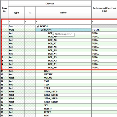
The Constraint Manager is where risk gets engineered out of the PCB layout, with electrical and physical limits configured so routing and placement stay inside fabrication and performance boundaries:
- Early error capture via real-time constraint checking during placement and routing
- On-demand DRCs with clear reporting and fast navigation to violations
- Constraint coverage for both electrical performance and manufacturing limits
Errors in libraries are one of the major root causes of manufacturing defects. We build and validate symbols and footprints so assembly is predictable and inspection issues are minimized:
- Validated schematic symbols and IPC-aligned footprint generation
- Property schema for lifecycle status, alternates, AML/AVL, and sourcing fields
- BOM outputs prepared for procurement and CM quoting workflows
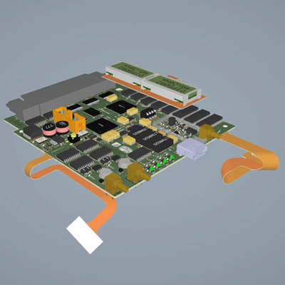
We generate manufacturing outputs from a controlled release process so fabrication and assembly expectations are explicit and repeatable:
A design is only "done" when it can be built consistently by your chosen manufacturer. We generate fab and assembly outputs directly from the Allegro database and align them to your CM’s preferred format:
- Gerber/ODB++/IPC-2581 artwork generation per CM/fab preference
- NC drill data, drill drawings, pick-and-place, and centroid outputs
- Export mechanical and draft layers with assembly and fabrication drawings, notes, and callouts
- BOM structure and supply chain data mapping suitable for procurement and CM quoting
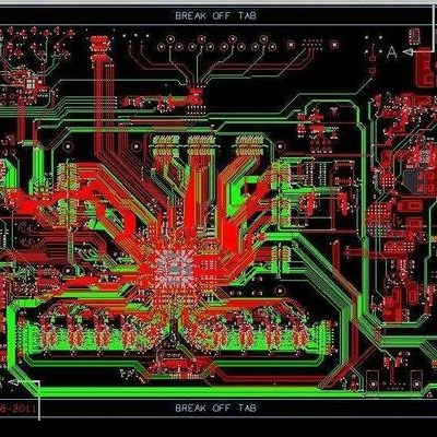
Our Work in Cadence OrCAD & Allegro
Power Electronics & Electrification
We help teams bring power electronics products to market that are stable, efficient, and ready to scale into production. Our work supports reliable power conversion, clean control behavior, and predictable performance in systems where switching noise, heat, and current density create the highest risk.
- High-current power stages (DC-DC, inverters, motor drives) with controlled current loops and thermal paths
- Power entry and protection (surge, inrush, filtering, isolation) aligned to safety and EMC expectations
- Mixed-signal control boards combining ADC/DAC, sensing, and embedded control around noisy power domains
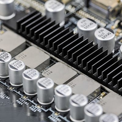
Industrial Systems and Automation
We support industrial product teams building electronics that stay reliable in the real world:on factory floors, inside heavy equipment, and in critical infrastructure. The result is hardware that tolerates electrical noise, survives long service lives, and integrates cleanly into complex industrial environments.
- Industrial controls and I/O electronics for automation, robotics, and process equipment
- Ruggedized embedded control for energy systems, grid infrastructure, and electrified equipment
- Sensor and communications hardware for factory monitoring, instrumentation, and condition-based maintenance
- EMC/ESD-aware designs for industrial environments with high switching noise and long cable runs
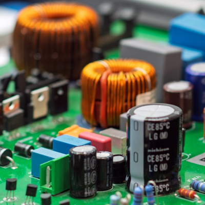
Defense & Aerospace Systems
We help defense and aerospace teams deploy rugged electronics that remain dependable under shock, vibration, temperature extremes, and electrical transients. Our solutions support mission-critical operation, long-term sustainment, and consistent performance in platforms where failure is not an option.
- Rugged embedded systems for ground vehicles, aircraft, spacecraft, and edge AI processing
- Mixed-signal control and sensing hardware designed for noisy environments and mission-critical reliability
- High-speed interfaces and dense interconnects constrained for predictable performance and low EMI sensitivity
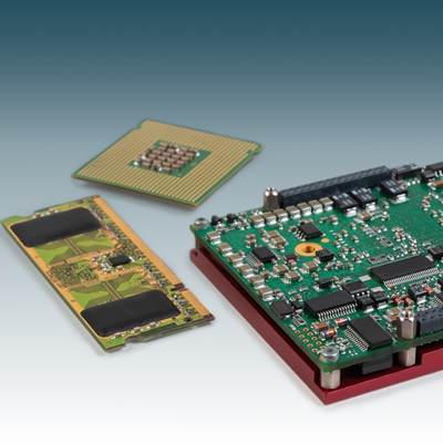
AI Data Center Infrastructure
We support AI data center hardware teams delivering infrastructure that operates reliably at high bandwidth and high power. Our solutions target dense networking and accelerator platforms where signal integrity, power delivery, and thermal limitations drive the success of the product.
- Networking and fabric hardware with dense high-speed connectors, retimers/PHYs, and controlled breakout geometry
- Accelerator and compute-adjacent cards requiring high-current power delivery, stable PDN behavior, and thermal-aware layout
- PCIe/CXL-class add-in cards with controlled channels, connector breakouts, and reference integrity
- High-current power delivery and VRM layouts aligned to transient loads and thermal constraints

Our Process
Our process is built around reducing risk before fabrication. We translate system requirements into layout constraints early, validate footprints and land patterns, and apply placement and routing practices that support signal integrity, power integrity, EMC, and manufacturability.
As the layout converges, we use targeted verification and DFM checks to catch the issues that trigger respins: invalid clearances, unstable return paths, high-density design decisions that don’t build, and stackup decisions that break impedance targets. The goal is simple: a first prototype that powers up cleanly and a design that is ready to scale to volume.
- Define requirements & constraints - Capture electrical, mechanical, safety, and compliance targets and translate them into OrCAD properties and Allegro Constraint Manager rule sets.
- Libraries & schematic capture - Validate symbols/footprints and complete front-end design in OrCAD Capture/CIS with part properties, net naming, and constraint hooks established early.
- Layout with continuous verification - Perform placement, planes, and routing in Allegro with real-time DRC/constraint checking; apply targeted SI/PI/EMI and DFM checks as the layout converges.
- Release a Manufacturing-Ready Package: - Generate artwork, drill, drawings, and assembly outputs (Gerber/ODB++/IPC-2581 as needed) aligned to your manufacturer’s requirements.
Additional PCB Design Software Support


Take Your Design Into PCB Manufacturing
Manufacturing is where cost and schedule are won or lost. We use Allegro’s manufacturing outputs, drawing utilities, and controlled export settings to deliver packages that match real fabrication constraints; quoting is faster and the design builds the way it was intended.- PCB manufacturing outputs - Fab/assembly files (Gerbers, IPC-2581, ODB++) generated from a controlled release process.
- Supply chain visibility - BOM structure and sourcing context prepared for procurement and CM quoting workflows.
- Standardized documentation - High-quality drawings and notes organized so fabrication and assembly expectations are clear.
- Guiding the design to production - We provide additional technical guidance needed to get the design quoted, or work with our CM partners.
Why Work With NWES?
- Broad expertise - We're a digitally-driven remote-first organization with diverse talent and experience. We know your technology because we've used it and built it.
- Manufacturing partners - We work with local and overseas CMs and EMS providers that are ISO-9001, AS9100, ISO-13485, IPC-A-610, NADCAP, and/or ITAR/JCP certified. We help you find the best option to produce prototypes and scale to volume production.
- Supply chain management - We take a proactive approach on projects to ensure your design can be produced at the required volume. We'll manage procurement from major distributors or brokers throughout your project.

Need a hand with a current or future PCB design project? Find out the difference our experts can make.
Contact us today for more information.
Our Clients and Partners



















