
Flex PCB and rigid-flex PCB designers are aware of the typical lack of ground planes in a flex design. Due to the lack of ground planes, and the obvious requirement of ground planes in high-speed PCBs and RF PCBs, one may think that flex PCBs cannot be used to support high-speed digital signals. However, even with a mesh or hatched ground plane, it is possible to design systems that include high-speed signals, both single-ended and differential.
Of course, there are limitations on the usage of hatched ground planes to support high-speed digital signals. For differential interfaces, the hatch has the potential to induce skew, but the superposition of the electromagnetic field from differential signals helps ensure lower noise. In contrast, single-ended signals without a nearby solid reference have the potential for greater radiated emissions from a flex PCB with a hatched ground plane.
In this article, I'll discuss some of the limiting factors for both single-ended and differential signals used in flex PCBs and offer some simulation data that illustrates bandwidth limits. There are also some simple estimators that can be used to determine when a hatched plane is no longer capable of supporting digital signals due to its periodic deviation in input impedance.
Hatched Planes and Input Impedance
In a flex PCB or on the flexible section of a rigid-flex PCB, a hatched ground plane can be used on one layer to provide some level of support for return paths. A hatched ground plane has a lattice structure, as shown below. The lattice structure is used so that the flexible region can repeatedly bend if required. It can be used on its own layer or in a coplanar configuration if needed.

Hatched ground plane in Altium Designer.
Because the hatched plane contains copper gaps in the latticework, a trace routed over a hatched plane will exhibit periodic variations in its input impedance. Although typically we do not do this, the magnitude and periodicity of the variations for a straight run of a single-ended or differential transmission line can be predicted from empirical models based on measurement data.
One way to quantify or index the expected variation in trace impedance over a hatched ground plane is to describe the plane using a fill factor. The fill factor of the structure can be defined as the ratio of the area occupied by copper to the area of a repeating cell or element in the hatched plane. Mathematically, we can express this as:

Fill factor definition for a hatched ground plane.
While an analytical model that uses the fill factor to predict impedance does not exist, one could develop an empirical model based on S-parameter measurements on a variety of flex PCB stackups. In addition, one should not expect the relationship to be linear due to the general nonlinearity of stripline and microstrip impedance. This applies to both single-ended and differential transmission lines.
Another factor to consider is variance in input impedance, which will be a function of frequency. Variation in the input impedance will depend on the fill factor, although this would vary to different degrees for single-ended and differential signals. The variation arises because the input impedance depends on the length of copper discontinuity due to gaps in the hatched ground plane.
At low frequencies, the hatched plane will resemble a solid ground plane because the impedance discontinuities appear to be very small when a signal wavelength is much larger than the impedance discontinuity. At higher frequencies, we would expect significant deviations in S-parameter plots when we compare a trace over a solid ground plane versus the same trace and termination over a hatched ground plane.
Single-Ended Transmission Lines
With single-ended traces, the trace impedance is determined by the distance to ground and the width of the trace. The copper weight also plays a role, but it is less important when the traces are much wider than the copper foil thickness. The channel bandwidth required for high-speed single-ended interfaces is quite small, topping out below 1 GHz for common serial interfaces. For an interface like DDR, which uses groups of single-ended traces, channel bandwidth per trace is still quite low in the GHz range.
This means that, although single-ended traces in serial interfaces like SPI do exhibit variation in the characteristic impedance, they tend to be more tolerant of the ground plane hatching due to the low channel bandwidth requirement. Gaps in the hatching pattern must be very large in order to be noticeable by a signal on an SPI bus, for example. If we take a typical load capacitance of an SPI bus of 30 pF, we can use the channel bandwidth limit to approximate the maximum gap size of the hatching pattern, assuming our impedance deviation demands a 20% limit on the size of the discontinuity. A very simple critical length calculation gives a rough estimate:
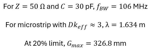
Example hatched ground plane maximum gap size estimation assuming a 50 Ohm target impedance
As long as the gap size is well below this maximum value, we likely do not need to worry about the signal integrity of the SPI bus, however this should be verified through testing on an oscilloscope. Note that this makes some broad assumptions, particularly the relation given the allowed impedance deviation the bus can tolerate, the limit this imposes in terms of a critical length, and the fact that the traces are already so short that the 30 pF load capacitance is limiting the rise time. On long flex cables, this third point may not hold at all. However, this gives us a very generous gap size allowance, which is much larger than what is typically seen in hatched ground planes.
What this does not address is the potential for radiated emissions when the bus is quite large or when there are many single-ended signals switching on the same bus. The ground plane hatching has some shielding effectiveness, which depends on the fill factor. A low fill factor might be fine for a single SPI signal, but it may admit too much radiated emission when a large number of SPI signals or GPIOs are routed over the hatched ground plane. This factor can only be accounted for in simulation or testing, or with empirical models from the research literature.
Differential Pairs
Differential pairs have an additional parameter that can be used to tune the impedance of the interconnect. That parameter is the spacing between the traces in the differential pair. Each trace functions as a return path for the other trace, and the spacing between them can be exploited to overcome a lack of ground below the differential pair.
This is quite important because differential interfaces can operate at multi-gigahertz speeds, which places the channel bandwidths in the multi-gigahertz range. While we don't expect extreme designs with 100G per lane routing on flex PCBs, some designs—such as sensor platforms or vision systems—definitely use interfaces with gigahertz channel bandwidth requirements. For example, JESD240 or MIPI standards might be routed on these PCBs, and this would require accounting for high channel bandwidth requirements.
An example S-parameter plot from one of my articles on the Altium Resources blog is shown below. This insertion loss plot is for a differential pair over a hatched ground plane and illustrates when severe losses start to arise due to the copper discontinuities in the hatched ground plane.
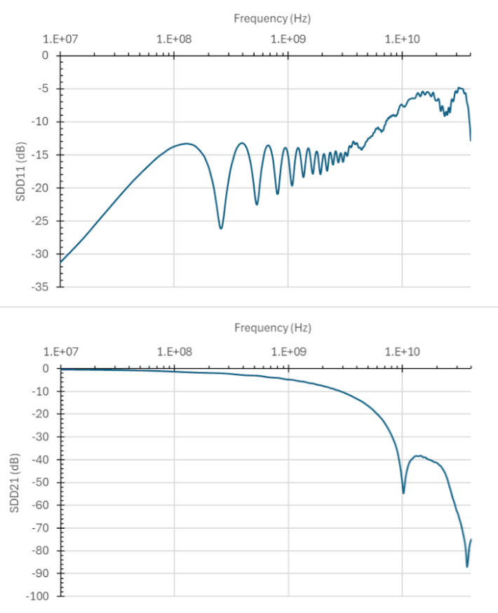
Example S-parameters for a differential pair over a hatched ground plane. Read the full article on Altium Resources
For differential pairs, these losses might be reduced or shifted in two ways:
- By changing the spacing between the traces in the differential pair
- By changing the hatch opening
- By changing the thickness of the flex substrate material
Decreasing the hatch opening size will push the frequency where insertion loss dips appear up to higher values. I have not investigated the effect of changing spacing and thickness on the frequencies of insertion loss, but I would expect that changing these values will only change the magnitude of those losses rather than the frequency. Due to trace-to-trace coupling in a differential pair, one would expect that decreasing the spacing will decrease radiated emissions and reduce the severity of insertion loss.
Front-End Flex PCB Analysis and Simulation
Before you start routing over a hatched ground plane in a flex PCB, a bit of front-end analysis can help estimate the appropriate hatch opening that will preserve signal integrity and still be manufacturable. If extremely small hatch openings are required for a very high-speed interface, a better option may be a cable that can carry the signal rather than attempting a flex design. Electromagnetic simulation software for PCBs can help validate this, or you can work with an experienced design firm to determine the best approach.
Whether you're designing high-speed PCBs for mil-aero embedded systems or a complex RF product, you should work with a design and development firm that can ensure your product will be reliable and manufacturable at scale. NWES helps aerospace OEMs, defense primes, and private companies in multiple industries design modern PCBs and create cutting-edge embedded technology, including power systems for high reliability applications and precision control systems. We've also partnered directly with EDA companies and advanced ITAR-compliant PCB manufacturers, and we'll make sure your design is fully manufacturable at scale. Contact NWES for a consultation.
Ready to start your next design project?
Our Clients and Partners


