
The Best High Speed Board Design Guidelines
By ZM Peterson • Feb 17, 2020These days, every device can be considered a high speed PCB. Older devices used slower edge rates, slower clock rates, higher signal levels, and higher noise margins. This placed less emphasis on things like impedance control, terminations, crosstalk, and power integrity. Newer devices are not so simple.
Today, any designer building a modern device for advanced applications should understand these points and should implement the right high speed board design guidelines. If you’ve never built a digital design using components with high edge rates, then fear not, there are some simple steps you can take to ensure signal integrity in your next board. Here are the important high speed PCB design guidelines to remember when working with fast edge rates.
Table of Contents
- What is a High Speed PCB?
- Impedance Control in PCB Design
- PCB Stackup Design
- PCB Return Path Design
- High Speed Routing Guidelines
- Power Integrity in High Speed PCBs
When Do High Speed PCB Design Rules Become Important?
A good way to check whether you need to concern yourself with high speed board design guidelines is to layout your new device on a breadboard or a development board. If you can layout your new device on a breadboard, and it works perfectly, then you can probably layout your board in any way you like and the finished PCB will still work. However, high speed devices generally won’t work on a breadboard. This is one reason component manufacturers release development boards for their components, particularly FPGAs, MCUs, RF components, and many other components.
If you can layout your peripherals on top of a development board, and the device works properly, then you can likely layout your new board however you like as long as you follow the stackup design in your development board. In this case, you should also pay attention to the signaling standards (SPI, UART, I2C, etc.) used in the board to ensure signals are not heavily degraded during routing. In many cases, you won’t be able to take such a simple approach, and everything will need to be integrated into a single PCB. In this case, you’ll need to pay attention to the following design points to ensure your high speed signals are not heavily distorted during routing.
What is a High Speed PCB?
When newer designers think about the term "high speed," they are likely to default to clock rate. However, a high speed design has nothing to do with clock rates and has everything to do with edge rate, or the rate at which the signal level swings between digital states. There is no clear delineation between high speed and low speed PCBs, and new designs with advanced components should be designed with high speed board design guidelines in mind.
In a high speed PCB, the rise time is fast enough that the bandwidth for the digital signal can extend into the high MHz or GHz frequencies. When this happens, there are certain signaling problems that will be noticed if a board is not designed using high speed PCB design rules. In particular, one might notice:
- Unacceptably large transient ringing. This generally occurs when traces are not wide enough, although you need to be careful when making your traces wider (see the section on Impedance Contorl in PCB Design below). If transient ringing is quite large, you'll have large overshoot or undershoot in your signal transitions.
- Strong crosstalk. As the signal speed increases (i.e., as the rise time decreases), capacitive crosstalk can become quite large as the induced current experiences capacitive impedance.
- Reflections off of driver and receiver components. Your signals can reflect off of other components whenever there is an impedance mismatch. Whether or not the impedance mismatch becomes important requires looking at the input impedance, load impedance, and transmission line characteristic impedance for an interconnect. You can read more about this in the following section.
- Power integrity problems (transient PDN ripple, ground bounce, etc.). This is another set of unavoidable problems in any design. However, transient PDN ripple and any resulting EMI can be reduced significantly through proper stackup design and decoupling measures. You can read more about high speed PCB stackup design later in this guide.
- Strong conducted and radiated EMI. The study of solving EMI problems is extensive, both at the IC level and the high speed PCB design level. EMI is essentially a reciprocal process; if you design your board to have strong EMI immunity, then it will emit less EMI. Again, most of this boils down to designing the right PCB stackup.
With these problems in mind, let's take a look at the important high speed board design guidelines designers should use to combat these signal integrity and power integrity problems.
Impedance Control in PCB Design
The term "high speed" refers specifically to the amount of time a digital signal takes to switch between OFF and ON states. Again, there is no specific rise time that dictates whether a board is in the low speed or high speed design regime. Generally, if the rise time of the signal is less than 5 ns, then you probably need to worry about high speed PCB design rules. However, we can get more granualar than this by looking at the signal velocity, the amount of time required for a signal to travel down an interconnect, and how this travel time compares to the rise time.
High speed boards are likely to have rise times that are shorter than the critical rise time in the board. This critical rise time depends on the critical length on an interconnect, which in turn depends on the allowed impedance mismatch at each end of an interconnect. I’ve discussed this in an article on Altium’s PCB design blog.
When your traces are too long, impedance control needs to be used, where your traces are routed with specified impedance. This is done by adjusting the geometry of your traces such that the impedance takes a target value. Even if you do not need to use impedance controlled routing, you should still apply termination between components when the sources and loads are mismatched. These days, components designed for very specific applications will include the relevant termination guidelines in your datasheets. Be sure to check your datasheets for guidance.

This USB board requires impedance controlled routing between USB PHY interfaces and connectors.
It's important to note here that, even if your interconnects are short compared to the critical transmission line length, you can still experience any of the other high speed signal integrity problems described in this guide. Don't think that simply using shorter traces will solve all of your problems. Many of the important high speed signal integrity and power integrity problems designers face in high speed PCBs can be solved simply by creating the correct stackup.
PCB Stackup Design
Your PCB stackup is a major determinant of signal integrity and power integrity. High speed signals require a nearby reference plane (power or ground) on an adjacent layer in order to ensure the loop inductance for that signal is low. I prefer to use a ground plane directly below the signal layer, followed by a power plane, but you can certainly use the power plane as the reference for a high speed signal as long as there is a ground plane on the next layer. This is true for digital and analog PCBs.
If you’re using interior layers to route signals, then it is best to avoid placing high speed signals on adjacent signal layers. Instead, separate these signal layers by ground and power planes. This will provide natural shielding between signals in your board, as well as shield them from external sources of EMI.
- Read more about stackup design for RF boards on our blog.
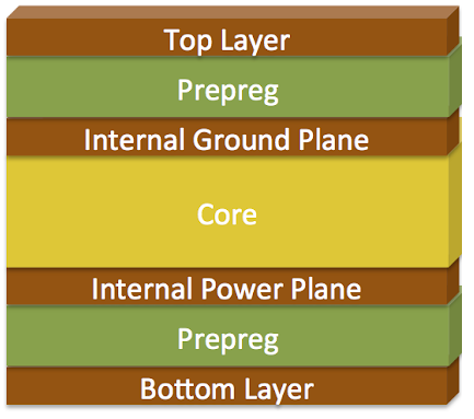
At minimum, you should use a 4-layer board for high speed PCB design. This is the typical stackup one would find in a 4-layer board for a high speed PCB. Advanced devices will use many more layers.
PCB Return Path Design
This is intimately related to stackup design, although it is one PCB guideline for high speed design that many designers ignore. In a real board, the return path taken by current in your board does not follow exactly below the trace carrying the injected signal. At high speed, the return current is more likely to be confined below the signal trace, but this is not the case at lower speeds. Take a look at this article for more information about PCB return path design.
Without repeating everything in the aforementioned article, I will list some important guidelines that will help prevent undue interference between signals, susceptibility to EMI, and power integrity problems:
- Don’t route over a ground plane gap. When designing your stackup, you may end up placing a gap in the ground plane to accommodate vias, mechanical holes, etc. Don’t ever route a high speed signal over this gap. By doing so, you increase the loop inductance for that signal. This then increases transient ringing, susceptibility and strength of crosstalk, and changes the impedance of the trace.
- Don’t route digital signals over an analog board section. Digital signals are relatively stable against interference from low-level analog signals as digital components are running at saturation. The same is not true for analog signals. In a mixed-signal board, a digital signal and its return current can induce strong crosstalk in an analog signal, which will greatly interfere with analog components. If you plan your board sections correctly, you shouldn’t have to worry about this.

Smart floorplanning can prevent interference between analog and digital board sections. Read more about this type of floorplanning here.
The high speed PCB floorplan shown above is designed for mixed signal boards to ensure analog and digital signals do not interfere with each other. By sectioning the different sections into different regions of the board, the different types of signals can be kept segregated from each other as long as the return path for each signal is correctly determined. This is actually much easier in high speed boards than in low speed boards as the return signal tends to follow beneath the trace carrying the injected signal, rather than taking a straight path back to ground.
High Speed Routing Guidelines
In addition to the impedance controlled design points mentioned above, traces should be carefully routed. Here are some of the important guidelines that will apply in any high speed PCB layout:
- Minimize use of vias. If vias are not properly designed, they can create an impedance discontinuity that causes reflections and attenuation. Ideally, the number of vias on an interconnect should be limited to no more than 2 in total.
- Use length equalization where necessary. For differential pairs, each end in a pair needs to have the same length within some specific tolerance. This is very important for ensuring that the receiver can cancel out common-mode noise on the interconnect. For single-ended signals, multiple signals may need to be routed in parallel (e.g., on a bus) such that the signals arrive at the destination at the same time.
- Prefer shorter trace lengths. Signals lose energy over time to dielectric absorption. This means you should opt to use shorter traces in order to minimize attenuation. Many signaling standards (e.g., LVDS and USB) will specify a maximum allowed PCB trace length.
- Pay attention to trace spacing. Signals should not be placed too close together in order to reduce the strength of crosstalk. Note that you can never eliminate crosstalk, but you can reduce it by placing the right amount of space between neighboring signals. Don’t trust the old "3W" rule here. Instead, run a crosstalk simulation in a simple layout to determine the right trace spacing.
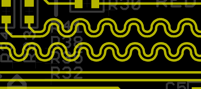
These curved sections are used for length matching between multiple differential pairs as part of an LVDS parallel bus. This prevents skew between multiple differential pairs.
One important point I’d like to add; with high speed devices (e.g., rise times of less than 1 ns), it is not a good idea to use orthogonal routing. This routing recommendation is still spread on many forums and by some "design experts." While this guideline may have been fine in years past, when digital devices tended to run much slower, this guideline should not be used in modern high speed PCBs. The idea behind orthogonal PCB trace routing is to eliminate inductive crosstalk. However, at high speeds, digital signal bandwidths reach into the GHz, and capacitive crosstalk between orthogonal traces will start to become noticeable. If you design the stackup correctly, then you won’t need to use orthogonal routing. I’ve discussed this in a recent article on Altium’s PCB design blog.
Power Integrity in High Speed PCBs
I've written about this multiple times on this blog, and PDN design is extensive enough to be given its own dedicated blog. Many books have been written about the subject, both for PCB design and IC design. For now, take a look at the blogs linked below as I’ve written about the important relationships between high speed PCB layout and power integrity in these digital systems (see below).
- PDN Design and Power Rail Ripple Suppression in Your PCB
- Causes of Ripple Voltage: Power Supply Noise and Transients in Your PDN
- Analog vs. Digital PDN Impedance: How to Design for Each Signal
- Remove Ground Bounce with Proper Bypass Capacitor Placement
One common problem in a poorly design digital board is a power drop when processor components are running at high clock rate. When multiple gates in a digital component switch, they draw significant current, and the fast current draw from a regulator creates a strong transient ripple on the PDN. This ripple can cause power to divert away from a selected component, which can then cause a component like an MCU or FPGA to switch off or reset. This problem, where a digital processor fails to run at full speed/clock rate is as much a decoupling capacitor problem as it is a stackup design problem.
The primary power integrity problem you'll need to confront in high speed PCB design is transient ringing on the PDN. This is a digital problem and an analog problem, although the problem is much more difficult to solve in the digital domain. For digital signals, the bandwidths are much wider than for analog signals, and the signals can span multiple resonances in the PDN impedance spectrum. The goal in PDN design is to judiciously select and place decoupling capacitors on strategic components in order to adjust the shape and peak heights in the PDN impedance spectrum.
The use of decoupling capacitors is the common gospel touted by most designers and is sometimes cited as the only way to combat power integrity problems in digital systems. However, once you look at the PDN impedance spectrum, you'll see that providing high interplane capacitance is the best way to keep PDN impedance low and smooth out PDN impedance peaks; note that this should be done in addition to the use of decoupling and bypass capacitors. In a high speed PCB, keeping the PDN impedance low will keep transient ripple on the PDN low. This, in turn, reduces phase noise (i.e., jitter) on the signals output from a component. While you can never completely eliminate transient responses on the PDN, you can reduce the strength of the transient response to where it does not cause large power drops and component failure.
The high speed board design guidelines I’ve presented here only scratch the surface. Working with advanced high speed digital designs requires plenty of planning and experience, and you should work with an expert design firm to create your next product. If you’re looking for a knowledgable firm that offers cutting-edge PCB design services and thought leadership marketing services for electronics companies, contact NWES today for a consultation.
Ready to start your next design project?
Our Clients and Partners


