
Most Common EMC Failures in PCB Design
By ZM Peterson • Aug 22, 2024Learn about the most common reasons for EMC failure in PCB design.
As the electronics industry advances, achieving electromagnetic compatibility (EMC) compliance is essential for successful product development. At NWES, we combine our expertise in EMC consulting with deep knowledge of PCB design to help you create systems that meet stringent regulatory standards. Whether it's reducing interference or enhancing signal integrity, we offer customized solutions for optimized performance. Collaborate with NWES to tackle the challenges of EMC compliance and bring your next PCB-based innovation to market with confidence.
During electronics product development, one of the most common reasons for product redesigns and PCB prototype re-spins is the failure of EMC testing. Governments around the world enforce EMC regulations for electronic devices, and these must be followed by product designers and manufacturers. Covered products include everything from radios to automotive systems, consumer electronics, and aerospace applications.
As most EMC problems originate in the design of a printed circuit board (PCB), a PCB design firm plays a critical role in ensuring compliance with EMC regulations. NWES provides EMI/EMC analysis services as part of its work with PCB design and manufacturing clients. We implement best practices in our designs, audit existing designs, and redesign PCBs for products that fail EMC testing. Our expert approach combines years of proven experience, partnerships with external testing consultants, and innovative software solutions to help clients solve their most difficult EMC challenges.
Before sending a PCB design for prototyping, an EMC review of the PCB is often necessary. We perform PCB design reviews focused on EMI in the PCB with the goal of identifying potential EMC testing failures. Our review process examines several critical aspects of circuit, PCB layout, and system-level design, including:

We often work with clients who have gone through multiple rounds of prototyping and EMC testing, only to see their devices continuously fail compliance. At this point, redesigns to the PCB are necessary, and these changes should be addressed by an experienced PCB design firm.
Based on a thorough review and assisted by innovative analysis tools, we identify the most effective design changes to suppress EMI problems. Our review covers all three levels of a design:
We offer PCB design services for a range of products, spanning high-speed digital systems, power systems, aggressive form factors, and RF devices. Upon completing a design review, we provide a detailed report outlining the required changes and a quote for the design updates. We use industry-standard enterprise-level PCB design software for all client projects.


![]()
![]()
EMC compliance remains one of the most challenging aspects of electronic systems design, and the journey does not end with a good PCB layout. We help you avoid expensive iterations by reviewing your design for the mechanisms that typically drive emissions and immunity failures, then recommending specific changes to your schematics, PCB stackup, component placement, routing, and grounding strategy.
Here's what you get from an EMC/EMI design review:
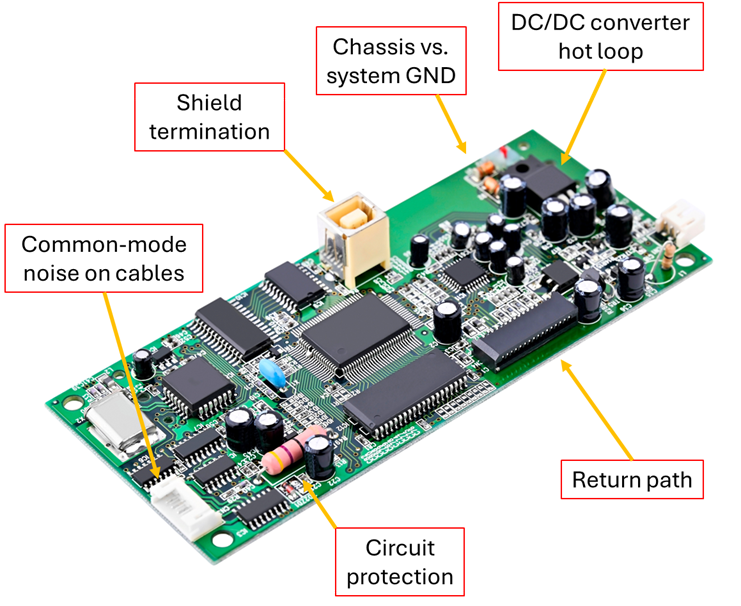
| Review Area | What We Look For | Output |
|---|---|---|
| Power Tree & Regulators | Hot loops, dV/dt nodes, input/output filtering placement, ground referencing | Marked-up schematic notes + placement/routing guidance |
| PCB tackup & Planes | Reference continuity, cavity resonances (risk), split/slot hazards, stitching strategy | PCB stackup recommendations + plane/return strategy |
| Critical Interfaces | Return transitions, connector breakout, common-mode sources, filtering misuse | Interface-specific routing rules + change list |
| I/O & Cables/Harness | CM current drivers, shield termination, pinouts that encourage radiation | Pinout/cable guidance + where to bond/stitch |
| Protection/Immunity | ESD/EFT injection paths, clamp placement, isolation gaps, resets | Protection placement corrections + layout constraints |
Once you're ready to put a product into testing, we provide referrals to EMC testing facilities through our partner network. For additional assurance, we also provide referrals to pre-compliance testing consultants who can identify any remaining system-level challenges, particularly those related to specific EMC regulations and standards.
Learn about the most common reasons for EMC failure in PCB design.

We always say to use solid ground planes in a PCB, but there are specific instances where split grounds are necessary.

Learn more about switching power supply noise in this article.


