PCB Design Review Services


Get Started

Expert Feedback, Precision Guidance

Following the incredible success of Zachariah Peterson's 1-Minute PCB Design Review series on the Altium Academy YouTube channel, we have received dozens of requests for design reviews. We have expanded this activity beyond technical content for our EDA software clients, and we are now offering comprehensive PCB design review services for client projects. We can provide this service to clients with quick turnaround under a flexible budget-based model.


What's Checked in a PCB Design Review

To get started, send us your high-level specification, PCB design files in your native ECAD format, and manufacturing outputs. Any relevant test results or simulation results detailing intended functionality can help expedite a design review and will assist us in providing the best course of action to improve the design.

  • Circuit design and component selection
  • PCB Stackup design and material selection
  • PCB layout and routing strategy
  • PCB footprints for common and specialty packages
  • Grounding system design
  • Factors influencing SI/PI/EMC
  • Your specification, design rules, and DFM constraints
  • Manufacturing outputs and drawings

Full turnkey design and manufacturing


Targeted Design Reviews and Analysis

Our PCB design review services align with our focused consulting services and allow clients to access expertise in more specialized areas. We offer multiple types of targeted design reviews for PCB projects:

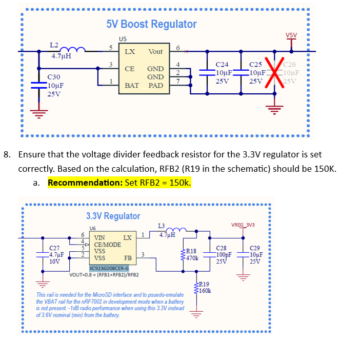
  • Schematic Design Review – A targeted review of circuit design and functionality, component selection, the PCB project library, bill of materials, and constraints defined in the schematics. This could include simulation work as part of the review process.
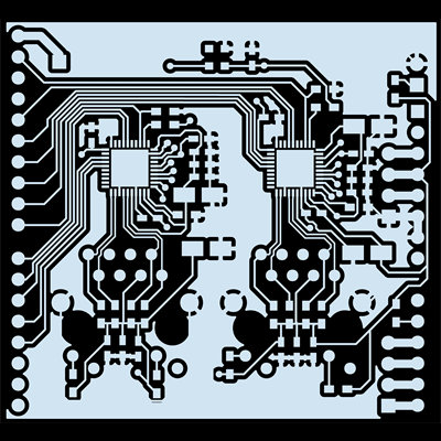
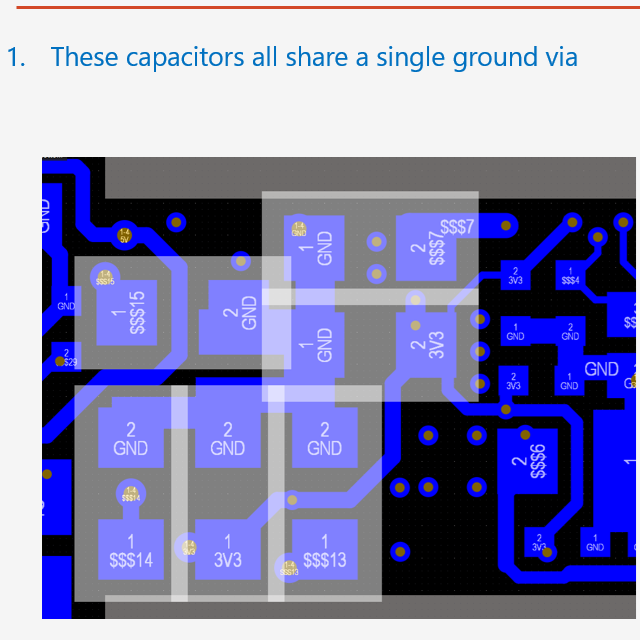
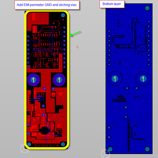
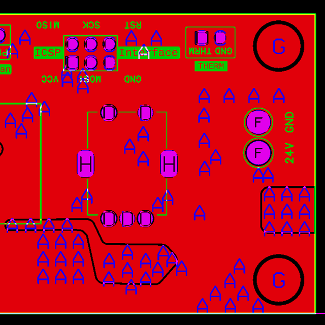
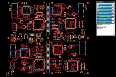
  • PCB Layout Review – A design review focusing on the PCB layout. We evaluate the stack-up, component placement, routing, and conformance to standard DFM/DFA constraints.
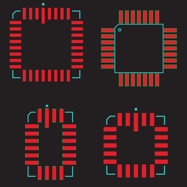
  • PCB Library Review – A check of the PCB footprints used in the design to verify they conform to the datasheet specification, common package geometry, and IPC standards.
  • PCB Manufacturability Review - An evaluation of the manufacturing outputs generated from your project, including fabrication and assembly files, to ensure compliance with industry standards and compatibility with vendor processes.
  • Signal Integrity Review – A deep dive into signal integrity for specific high-speed or RF interconnects using industry-standard simulation tools. Visit our Signal Integrity Consulting page to learn more.
  • EMC Design Review – A review of the schematics and layout with a focus on compliance with EMC standards and regulations. Visit our EMC Consulting page to learn more.

Once we have completed the review of your project files and your manufacturing outputs, we provide a comprehensive report with the results. This includes suggested changes to the circuit design, PCB layout, and routing. More specialized points, such as SI and EMC, are also addressed in the final report where applicable. This may include results from simulation or analysis software and a validation of the required design changes.


What's In a Review Report?

The goal of a PCB design review report is to give you a clear, prioritized path from "here’s what we found" to "here’s what to change." Each item above is written as actionable guidance (with marked-up files and screenshots where helpful), so you can implement the highest-impact fixes first, reduce risk before fabrication, and move into build and test with fewer surprises.


Related Resources


cover image

A PCB DFM Checklist Helps You Pass a Design Review

By ZM Peterson • Jan 15, 2020

Here's how a PCB DFM checklist will help you pass a design review before manufacturing.

cover image

Your PCB Layout Review Checklist Before Manufacturing

By ZM Peterson • Nov 18, 2020

Before you send your PCB out for manufacturing, run through a PCB layout review checklist to ensure manufacturability and conformance to design requirements.

cover image

What to Keep in Your PCB Footprint Checklist

By ZM Peterson • Sep 10, 2020

Before you start your PCB layout, look through the items in our PCB footprint checklist to help you stay on track.



Our PCB Design Review Process

We provide customers with PCB design and advanced packaging design solutions to accelearte the innovation process for cutting-edge electronics.
  • Contact us for a consultation and quote.

  • Send us all available design data in your native ECAD software file format, as well as your manufacturing files and applicable test/simulation results illustrating core functionality.

  • We'll review your schematics, PCB layout, library, BOM, and manufacturing files to identify anything that compromises basic functionality, SI/PI/EMI, manufacturability, and reliability.

  • At the conclusion of the review process, we'll provide a comprehensive report outlining the findings and proposed changes to the design which will improve the final product.

How We Work

Why Work With NWES?


  • Broad expertise - We're a digitally-driven remote-first organization with diverse talent and experience. We know your technology because we've used it and built it.

  • Manufacturing partners - We work with local and overseas CMs and EMS providers that are ISO-9001, AS9100, ISO-13485, IPC-A-610, NADCAP, and/or ITAR/JCP certified. We help you find the best option to produce prototypes and scale to volume production.

  • Supply chain management - We take a proactive approach on projects to ensure your design can be produced at the required volume. We'll manage procurement from major distributors or brokers throughout your project.


Get Started


Need a hand with a current or future IC substrate design project? Find out the difference our experts can make.


Contact us today for more information.


You may include a ZIP file with your request (25 MB maximum)


Ready to work with NWES?
Contact us today for a consultation.

Contact Us Today

Our Clients and Partners