
Switching Power Supply Noise, Radiated EMI, and EMC
By ZM Peterson • Jan 24, 2022Learn more about switching power supply noise in this article.

Northwest Engineering Solutions provides power electronics design services for systems that must meet tight efficiency, EMI/EMC, thermal, and safety requirements. We design and review power conversion and control hardware spanning DC-DC power stages, gate-drive and sensing circuitry, isolation boundaries, and even mixed-signal interfaces that connect power circuitry to digital control.
Our workflow is built to take a design from early architecture through schematic, PCB layout, and a complete manufacturing package. You get actionable design outputs—component selections, layout constraints for high di/dt loops and switching nodes, creepage/clearance planning, and DFM-ready documentation—so prototypes behave like production hardware and scale cleanly to volume builds.
Modern power electronics designs push higher power density, faster switching edges (GaN/SiC), tighter EMI limits, and smaller mechanical envelopes, all while demanding higher reliability. Success comes from treating the power stage, sensing/control circuitry, and PCB layout as one coupled system, with clear constraints for switching loops, return paths, isolation barriers, and thermal spreading.
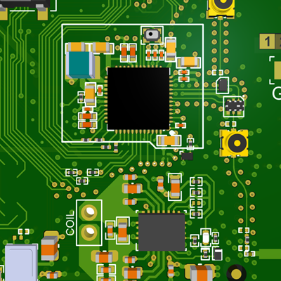




Power electronics layouts fail for predictable reasons: parasitic inductance in hot loops creates ringing and overshoot, switching nodes capacitively couple noise into control and I/O, sensing gets corrupted by return path errors, and isolation boundaries get compromised by placement or routing shortcuts. The goal is to lock down the constraints that govern switching behavior, measurement integrity, EMI performance, and safety margins before the first prototype is built.
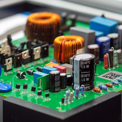
We serve multiple industries and markets with advanced electronic systems operating in demanding environments.
Whether you are building a one-off prototype or preparing for volume production, we align the electrical design with your mechanical constraints and manufacturing plan. That includes component availability, PCB/material constraints, inspection requirements, and practical build notes so the design can scale without surprises.
Some power electronics design requirements in contemporary application areas are outlined in the table below.
| Application Area | Typical Design Priorities |
|---|---|
| Motor Drives and Inverters | • Stable control across load transients and operating conditions • dv/dt management to protect insulation and reduce EMI • Current measurement integrity for control and protection • Thermal design for power devices, magnetics, and mechanical mounting |
| Industrial Power Supplies and Converters | • High efficiency across the full load range • Predictable EMI/EMC performance at the system boundary • Isolation strategy with appropriate creepage/clearance margins • DFM/DFA alignment for repeatable builds and testability |
| Battery Systems (Chargers, Power-Path, BMS) | • Accurate sensing and stable references in a noisy environment • Protection coordination for fault handling and safe shutdown • Low standby power and robust sequencing/monitoring • Connector and harness considerations for conducted/common-mode noise |
| Automotive and Transportation Power | • Wide input range and transient immunity • EMI robustness with long cables and shared grounds • Thermal cycling and reliability in harsh environments • Design constraints driven by packaging and serviceability |
| Aerospace and Defense Power Conditioning | • High reliability and derating-driven design margins • Isolation and safety practices aligned to program needs • EMI control with sensitive RF/avionics subsystems nearby • Documentation and traceability expectations for builds |
| Test and Measurement Power Platforms | • Low-noise rails for precision analog and mixed-signal loads • Fast transient response without measurement corruption • Layout practices that keep noise predictable and repeatable • Serviceability and clear test access for validation |
Learn more about switching power supply noise in this article.

A power supply ground region needs to be clearly defined, both on and off your PCB.

GaN vs. GaAs: which type of amplifier is right for your application? Here’s what you need to know about these semiconductors.




















