
Your Guide to High Speed Signal Integrity in PCBs
By ZM Peterson • Jun 30, 2020When we talk about high speed signals, we have a very specific meaning. High speed PCBs carry signals with very fast rise times, typically with ECL, CMOS, or other logic families. These systems are meant to run at high clock and data rates, and sometimes with multilevel signaling.
If you’re designing a high speed PCB, then you need to know everything you can about high speed signal integrity in your PCB layout. A comprehensive view of high speed signal integrity requires some heavy math, and even prominent signal integrity engineers actually ignore the math required to fully understand and analyze high speed signal integrity. If you need to catch up on the finer points of high speed signal integrity or you’re a new designer in the field, keep reading to learn more.
Common High Speed Signal Integrity Problems
To get started, the only thing that separates high speed from low speed signals is the signal rise time. There is no specific frequency or signal rise time beyond which a PCB would be considered to run at high speed. The clock frequency has nothing to do with high speed signal integrity, although it is true that signals with higher repetition rates tend to have faster edge rates. In fact, all the high speed signal integrity problems I’ll discuss here happen in every PCB. The difference is that, at lower signal rise times, these signal integrity problems are so minor that they might never be noticed, and the low speed system you build will probably work fine no matter how you create your PCB layout.
There are some common problems that only become obvious once a system begins running at high speed. With that being said, the points I’ll discuss here are well-known in high speed electronics. Here are the important high speed signal integrity problems to consider in your next digital system:
Before we jump into these areas, it’s important to understand one of the factors that causes these effects at high speed/high frequencies. One of the most important factors is dispersion in the PCB substrate. This refers to the fact that any material has different levels of loss and different refractive index at different frequencies. In other words, the speed of light and absorption both vary with frequency due to the atomic/molecular structure in the PCB substrate.

Dispersion is the source of some high speed signal integrity problems and needs to be considered during high speed signal integrity analysis.
This will become important once we look at signal reflection, signal distortion, and crosstalk. It also plays a role in the fiber weave effect, although this is normally examined well beyond the digital domain. Now that we’ve got a vague idea of what qualifies as a high speed signal and a high speed PCB, keep reading to learn more about the potential high speed signal integrity problems I outlined above.
Signal Reflection
Reflection at impedance mismatches can lead to ringing in an interconnect, where the signal exhibits a damped oscillatory transient response at each reflection. This term "ringing" is sometimes used to refer to a stair-step response in the signal level seen at the driver, which occurs when reflection causes a phase reversal.
The cure here is to always impedance match your driver, interconnect, and receiver in a high speed interconnect. The use of a via on an interconnect creates two sections of transmission line, each of which will need to be impedance matched to the appropriate value. A real transmission line network with a reactive load component can create a network with a complex input impedance spectrum, which also needs to be considered when designing an interconnect for high speed signals.
Then when we consider dispersion, copper roughness, and skin effect losses, the impedance of a line can be a very complex function of frequency. The result is that it can be difficult to perfectly match the input impedance spectrum of a circuit to the transmission line impedance without careful geometric adjustments. The example impedance spectrum shown here is for a stripline matched to a 50 Ohm receiver with ~10 pF input capacitance. With careful geometry optimization, I was able to get the impedance deviation to be less than 1 Ohm throughout the signal bandwidth with ~3 dB per inch insertion loss at 1 GHz.

Impedance matching through interconnect geometry optimization allows careful matching throughout the signal bandwidth.
These results can be produced in a typical field solver, or you can use an optimization technique to determine the geometry that minimizes deviation from a target impedance.
Signal Distortion
Signal distortion occurs when a signal travels to the end of an interconnect, and it does not have the same shape as it did when it was injected into the interconnect. This occurs due to dispersion, which causes different frequency components in the bandwidth of a digital signal to travel at different speeds and experience different levels of loss.
The end result of signal distortion is two-fold:
- Spreading of the signal in the time domain due to the velocity difference between various frequency components.
- Greater insertion loss along an interconnect at higher frequencies.
The first point above causes a signal to appear stretched at the receiver; this stretching is greater when the interconnect is longer. The second point occurs because real transmission lines act like low-pass filters, both due to dielectric losses and resistive losses. Eventually, at sufficiently high frequency, absorption and scattering can occur as a signal propagates, which increases losses in specific frequency bands (both aspects are complex mathematics problems for inhomogeneous anisotropic media like PCB substrates). Both aspects are a reason why a shorter interconnect is preferred when possible.
Crosstalk and Coupling
Crosstalk is a simple phenomenon to understand; a replica of the rising edge of a signal is superimposed in a neighboring channel. A faster signal rise time leads to more intense crosstalk. Again, this does not depend on the data rate or clock rate. When crosstalk is excessive, the signal on the victim line can exceed the noise margin at the receiver, causing the signal to fall into the undefined region. This then causes the eye diagram to close, leading to higher bit error rates in the affected channel.
Coupling is essentially the same thing as crosstalk, and it occurs via the same mechanisms (parasitic capacitive and inductive signal transfer between conductive elements in a PCB layout). When we refer to coupling, we are basically referring to signal transfer to an element in a PCB other than a victim trace.

Signals in a failed DDR4 channel. The differential crosstalk on the rising edge is too high, leading to excessive overshoot in the transient response seen at the receiver.
Ground Bounce
Ground bounce can be easily confused for crosstalk as it can produce a momentary peak in the output signal level from a driver IC. Ground bounce, also known as simultaneous switching noise, occurs when transistors in an IC switch. The parasitic inductance on the bond wire leading back to ground creates a back EMF as current rushes into the IC. This causes the signal level seen by the receiver to appear smaller as the ground potential appears higher when measured between the output and the ground pin.
Because ground bounce is caused by a parasitic inductance, and because there is some parasitic capacitance at the ground pin or pins on an IC, ground bounce can have an LC resonance. This would produce the same type of transient response shown above for the failed DDR4 channel. This is one reason why it can be difficult to distinguish crosstalk from ground bounce without some precise measurements or high speed signal integrity simulations.
Analyzing High Speed Signal Integrity
When we say "analyzing" high speed signal integrity, we’re really referring to a number of tasks. All these tasks focus on the behavior of digital signals in the time domain. In many systems, you know the response of an element on your PCB, such as a transmission line, only in the frequency domain. In other cases, you have a time-domain measurement, but you’d like to know the behavior of the system in the frequency domain. For this reason, we need to often use a Fourier transform (or its inverse) to take measurements in one domain and convert them to the other domain.
The most advanced models for high speed signal integrity analysis are causal models. These models enforce a Kramer’s-Kronig relation between the real and imaginary parts of some aspect of the system, such as the PDN impedance, transmission line transfer function, dispersion in the PCB substrate, or a circuit’s response in general. These models have always been the subject of signal processing and signal modeling research, and the number of causal models for different situations is too long to discuss in this article. Take a look at the research literature if you want to learn more and find causal models for your system.
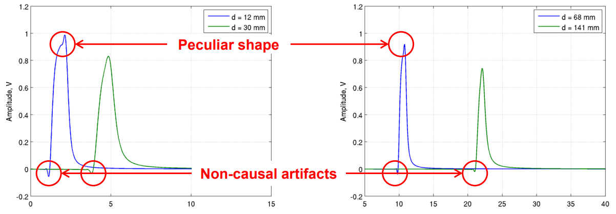
This figure from the IEEE P802.3bj Task Force (2014) shows noncausal signal behavior in an interconnect, revealing the importance of high speed signal integrity modeling.
What About High Frequency Signal Integrity?
In some ways, high frequency signal integrity is easier than high speed signal integrity, and in some ways they are not at all comparable. In high speed signal integrity, we pay attention to what happens to signals in the time domain. Frequency content for a digital signal is spread out over a large range of frequencies; if you look at a very fast digital signal (e.g., ~17 ps/V slew rate), the bandwidth of this digital signal spreads from the clock frequency out to infinity with a sinc envelope defining the amplitude of its harmonics. In high-speed PCB design where data rates exceed ~1 Gbps, the job of the PCB designer is to design channels such that they provide more bandwidth than the receiver's minimum bandwdith requirement. This will allow the receiver to recover data from a digital signal as it arrives at the receiver.
Analog signals have much lower bandwidth, which might have frequency components spread over less than an octave. At high frequency, you’ll see the same effects discussed above, but they’ll appear within a smaller frequency band. In some ways, this makes design easier, particularly transmission line design and PDN design. However, high frequency analog signals typically run at much higher frequencies than the high end of a digital signal. This creates new signal integrity problems that are not always visible in today’s modern high speed digital systems.
As your operating frequency increases well beyond 20 GHz, the first point you’ll start to notice is higher dielectric and absorptive losses. Second, copper roughness becomes more critical due to the skin effect, where current is concentrated around the outer edge of a conductor. Another signal integrity problem that occurs at high frequencies is the fiber weave effect, where resonances in fiber cavities induce skew (phase noise or shifts), additional losses, and radiation from cavity resonances.
We also haven’t said much about power integrity aside from ground bounce, which is another important aspect of high speed digital design. If these problems seem insurmountable in your system, you might need the right design firm to help you create a high-quality PCB layout for your next digital system.
At NWES, we know how to spot high speed signal integrity problems in your PCB layout and how to analyze signal behavior in your system. We’re here to help electronics companies design high speed, high frequency, and high density PCBs for a variety of applications. We know how to keep your designs operating properly while helping you stay within budget. We've also partnered directly with EDA companies and advanced PCB manufacturers, and we'll make sure your next layout is fully manufacturable at scale. Contact NWES today for a consultation.
Ready to start your next design project?
Our Clients and Partners


