
RF PCB Layout and Routing Tips for mmWave Products
By ZM Peterson • Sep 30, 2020Digital systems are pushing ever further into the mmWave regime, and more designers will need to start understanding how to accommodate high frequency analog signals on digital boards. This is meant to provide wireless functionality in IoT products, mobile products, robotics, and other application areas. Digital designers also need to learn something about signal integrity at RF frequencies as digital signal bandwidths push well into the 10’s of GHz range.
Whether you’re a digital or high frequency analog designer, it pays to know how to work with mmWave frequencies and how to accommodate RF signals in a digital design. RF PCB layout is all about preventing interference between board sections and ensuring sensitive signals do not heavily interfere with each other. If you’re unsure how to get started with a new RF product, including at mmWave frequencies, take a look at our RF PCB layout tips.
Component Placement
Before you start routing anything, you need to place components around your new PCB. This is where smart floorplanning becomes critical; you need to place components and circuit blocks so that EMI between them is minimized. Simply brute-force filtering every signal around the board isn’t going to guarantee signal integrity, and there are more elegant ways to floorplan an RF PCB layout to ensure signal integrity.
There are four primary tasks to undertake when preparing an RF PCB layout:
- Stackup design. Just like high speed boards, RF boards need to have the right stackup. This helps provide stable impedance, plan routes, and provide isolation from external EMI.
- Impedance control and routing style. Stackup and impedance control go hand-in-hand, and many high frequency boards operating at microwave or mmWave frequencies will need impedance controlled routing. The stackup will determine your trace width for your desired routing style, and circuit blocks should be arranged with enough space to accommodate the routing style in the PCB layout.
- Circuit block arrangement. When you’re planning your RF PCB layout, but before you start routing, try to segment circuit blocks into different sections of the board. This can be done by function or frequency, as shown in the accompanying floorplanning image. Watch out for planning your return path in the board as you do not want analog signals with different frequencies and modulation schemes interfering with each other.
- Planning for isolation. Unless you’re using an inherently shielded waveguide routing style like substrate integrated waveguides, you’ll need to plan isolation into your PCB layout.

This type of circuit block arrangement in a PCB layout is typical in mixed signal products and will work at mmWave frequencies.
In the above layout, the important point here is the use of isolation between different circuit blocks and the placement of an antenna section near the board edge. As an example of a commercial mmWave system, the center-fed patch antenna arrays used in 77 GHz radar modules are placed on a separate board, so the antenna board’s ground plane and ground pour provide the required isolation from other board sections. Once you’ve determined where you should place each component in your layout to ensure signal and power integrity, you can start to think about routing your RF PCB.
Routing Your RF PCB Layout
Just like a high speed digital board, RF PCB layout and routing requires preventing a range of standard signal integrity problems, which becomes quite important in both high speed and RF systems. The same problems that arise in high speed PCBs will also occur in an RF PCB layout, the difference is the relevant frequency range, bandwidth, and sensitivity to noise. When you’re floorplanning your PCB layout, you’ll have to plan on routing and isolating critical RF lines to prevent interference between them. This involves isolating routes and ensuring consistent impedance along a route.
Transmission Line Styles
Transmission line styles used in RF PCBs are the same as those used in routing for any digital PCB. These are microstrip, stripline, and coplanar waveguide. The difference is that RF PCB layouts are de facto single-ended, except in some cases where a differential RF driver and receiver interface can be built with two out-of-phase signals being driven on the pair. Off-the-shelf components used in RF PCBs do not operate in this way.
The three main transmission line styles and their usefulness in RF PCB layout and routing are summarized below. In this table, I’ve summarized the main advantages of these three types of transmission lines in terms of linewidth and losses.

In an mmWave PCB, the primary transmission line structure used to route signals is a grounded coplanar waveguide. This structure uses a standard coplanar arrangement with a via fence around the structure. The via fence along the interconnect is precisely designed to provide high-frequency isolation that suppresses frequencies below a particular cutoff from interfering with the propagating signal. Conversely, the same via fence also isolates the mmWave signal from radiating strongly and then interfering with other signals in the board.
The downside of a via fence along an mmWave PCB interconnect is that the via fence limits the interconnect’s bandwidth. This leads to a point where the impedance spectrum becomes mismatched from its target impedance (normally 50 Ohms), and you will see a peak in the S11 spectrum. This will signify the limit of quasi-TEM propagation and the end of the quasi-static approximation in the transmission line. Above the first cutoff, mode propagation begins and periodic dips will appear in the S21 spectrum for the interconnect.
A design example prepared in Altium Designer is shown below. In this example a coplanar waveguide is placed coming into a connector transition with 2.042 mm via spacing across the waveguide. This waveguide was built on a 30 mil RO4350B laminate. This example line was used for a connector interface on a test board with very good results at short-range radar frequencies. The cutoff of the quasi-TEM mode is at approximately 42 GHz and is found by matching the lateral spacing between vias to the half-wavelength of the propagating signal (don't forget, we need the effective Dk value for this!).
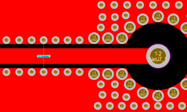
Example grounded coplanar waveguide built on 30 mil RO4350B. The cutoff for this particular transmission line is at about 42 GHz.
The following link provides much more information on grounded coplanar waveguide design, including equations that are applicable in the quasi-static limit and more results showing bandwidth limiting and power loss in general.
Finally, to get some more tips on routing in RF PCBs, take a look at our other blog post on this topic (linked below). In particular, there is a figure comparing losses across frequency in somewhat long interconnects which supports the broad advantages/disadvantages outlined in the table above.
Vias in RF PCB Layout
The use of vias in RF PCB layout should proceed with caution. There are a number of points to consider when determining whether to use vias in your PCB layout, but the most important point is the signal frequency. Just like other areas of RF layout, you might need to sacrifice routing convenience in favor of RF signal integrity.
At sufficiently low frequencies, vias on an RF transmission line may not be so important as their input impedance resembles the impedance of the downstream section of transmission line. Assuming all downstream sections are matched, then we don’t need to worry about the impedance of a via. This changes when we look at high frequencies, particularly at mmWave frequencies. The image below shows where parasitics arise in the use of vias in mmWave routing in an RF PCB layout.

When routing mmWave signals through vias, it is advised to backdrill the via transition to prevent distortion and reflections. To set the impedance to a target value, stitching vias must be placed around the signal via to control parasitics.
The approximate cutoff where the impedance of a via starts to significantly deviate from its target impedance is above approximately 3 to 5 GHz. Above these frequencies, most via calculators you will find online will fail to give correct results. They will fail in a few key ways.
- They predict that via impedance is constant, which is totally untrue; via impedance is always a function of frequency, initially appearing capacitive and then inductive in the quasi-static domain.
- They tend to overestimate propagation delay, which leads to totally incorrect estimates of phase delay in an interconnect. At mmWave frequencies involving phase matching (e.g., phased arrays for beamforming), you need to know the delay to compensate phase mismatch.
- They do not account for stitching vias, which are required to set the impedance of a via transition structure to a target value. Stitching vias are an important tool that can be used to enable through-hole vias at mmWave frequencies.
An example of a real via transition that is appropriate for use at 68 GHz is shown below. I’ve shown this particular example in several presentations because it illustrates the real impedance of a via at very high frequencies.

Return loss spectrum for a via with stitching vias and grounded coplanar waveguide feedlines.
From this return loss graph, we see that the impedance of the via structure (assuming infinitely long feedlines) is only near 50 Ohms right at approximately 68 GHz. We can also see that the via transition has very high Q value. The popular transmission line calculator applications you find online, and even some you purchase from well-known ECAD vendors, can’t predict this behavior and will always give wrong results. This is something that can only be correctly predicted with an electromagnetic field solver.
Isolating RF Sections While Routing
Many isolation structures have been developed and examined over the recent past, particularly as mobile devices became more ubiquitous and started operating at successively higher frequencies. Now that mmWave products are becoming more common and widely commercialized, designers need more isolation structures than just taking advantage of guard traces and ground planes in a multilayer board. Some options include:
- Electronic bandgap structures. These are prevalent in mobile devices, boards with antenna arrays, and other passive RF products.
- Via fences. This is a variation on electronic bandgap structures, where a periodic via array provides narrowband suppression of RF radiation through destructive interference.
- Ground pour. This is standard in many boards, but it is also useful in RF boards as it allows a designer to use coplanar waveguide routing. By adjusting the dimensions of the line and its distance to ground pour, a designer can maintain quasi-TEM propagation.
- Absorbing conformal coatings. The use of absorbing conformal coatings on a PCB can provide wideband isolation. In particular, it suppresses edge emission from cavity modes at mmWave frequencies, which can have a complicated structure with non-integer relationship between resonances.
The routing style you choose can have some natural isolation, which is why mmWave PCBs will often use grounded coplanar waveguide routing. Alternative methods are substrate integrated waveguides and mode-selective transmission lines, both of which provide high isolation. Critical traces at mmWave frequencies should use one of these advanced routing schemes as well as isolation techniques to prevent interference between board sections.
The experienced PCB design and layout team at NWES can help you create your next advanced RF PCB layout with advanced routing schemes. We help our private clients, aerospace companies, and the US military stay at the cutting edge with advanced PCB design and layout services. We've also partnered directly with EDA companies and advanced PCB manufacturers, and we'll make sure your next design is fully manufacturable at scale. Contact NWES for a consultation.
Ready to start your next design project?
Our Clients and Partners


