Can You Trust a Standard Stackup From a PCB Fabricator?
By ZM Peterson • Aug 13, 2024PCB fabrication houses often provide a standard stackup option that can help you quickly design a variety of circuit board layouts.
PCB manufacturing is a multi-step process that begins with the conception of a product and culminates in a ready-to-assemble PCB. The standard PCB fabrication process is one of two steps in PCBA manufacturing,where a circuit board's design data is converted into a physical structure as per the provided design specifications. The steps involved in the fabrication process depend on the complexity of the PCB, and it is important not to skip any step for optimum performance of the final product.

All printed circuit boards are built on some base materials, with epoxy-filled fiberglass being the most commonly used substrate. However, certain applications require flexible PCBs, and accordingly their substrates are made up of easily bendable materials like polyimide or Kapton plastic. Other applications like RF PCBs will require PTFE base materials to support low-loss signal propagation, or metallic substrate PCBs may be needed for high-power systems.
The PCB fabrication process begins with the transfer of design data from design files to the printed circuit board. The purpose in this step is to etch away copper from the base materials, leaving behind conductive copper elements that make up circuits in the PCB. Printing processes can be broadly classified into two categories:
Photo tooling is a conventional method of transferring the circuit design from a file to a film (stencil). A special printer, called a photoplotter, is used to create films that are then used to transfer copper circuitry to the board. Photoplotter technology provides a high-definition film of the printed circuit elements through extremely precise printing. A photo-negative image is printed on a clear plastic sheet in black ink, and this sheet will act as a mask for exposing a photoresist material coated on the copper.

Usually, the clear portion of the sheet represents the non-conductive portion of the PCB while the black-ink printed design corresponds to the conductive copper area. This is the standard followed for the inner layer of PCB. Printing of the outer-layer films follows the opposite convention: the black portion refers to the part that will be etched away while the clear portion represents the copper area.
In the case of LDI, circuit patterns can be transferred directly onto the PCB using a precisely focused computer-controlled scanning laser beam. This technique is highly precise and does not have any alignment issues that are typically associated with photoplotter tooling methods. Furthermore, photo films typically need to be replaced periodically as they degrade over time. Laser direct imaging does not have this problem as it does not require a medium to transfer the image to PCB.
A laminate material with pre-bonded copper is coated with a photoresist material, and this photoresist layer is exposed to ultraviolet light through the printed layer film. In the case of the direct imaging technique, a laser beam is used instead of UV light. This optical exposure results causes the photoresist material to harden into a pattern that matches the copper circuitry. The rest of the area is still pliant and is easily removed with chemicals. The unwanted copper portion is removed from the board through an etching process, leaving behind the printed circuitry pattern that was blocked with the hardened photoresist. The PCB is finally washed with chemicals to remove the photoresist before transferring the board to the next phase.

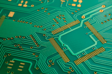
Multi-layer PCBs consist of multiple layers stacked on top of each other. After all the layers have been cleaned and prepared, alignment punches are used to ensure there is no misregistration between layers. Registration holes are used to align the inner layers with the outside layers. A machine called an "optical punch" is usually used for this purpose.
The next step is to ensure the inner circuit board layers were fabricated as intended in the design database, so the PCB enters an inspection phase. Automated optical inspection is a popular method of PCB inspection as it can be used to identify fabrication defects. This method involves using a computer to automatically examine the inner layers for incomplete designs or remaining resist material. Once the PCB has passed inspection, it moves on to the next phase.
A press machine is used for aligning, heating, and bonding the layers together with copper foil and insulating material between them. The insulating material is usually fiberglass pre-impregnated with epoxy resins., also known as "prepreg." Heat and pressure from the lamination process melt the resin in the prepreg, which will fuse together with the other layers in the PCB stackup as the resin cools. If your board is sent to a fabrication shop, the fabricator will typically use copper-clad laminates from a materials vendor.

Once the PCB is printed, etched, washed, and laminated, the next step is to drill holes for mounting components. For a multilayer printed circuit board to transmit signals from one layer to the next, via holes must be drilled or laser-cut to connect between layers. Numerical drill data prepared from PCB design data is used to indicate drill locations, and the drill spots are precisely located using an X-Ray machine. The PCB stackup is secured before drilling using guiding or tooling holes on the PCB panel.
After drilling and debris removal, the next step in the PCB fabrication process is application of copper plating deposition on the outer layers. This involves exposure of the PCB to various electrolyte solutions, during which time copper will build up connections along via holes and the exposed copper.
Outer layer imaging is done with the same techniques as the inner layers. A photoresist material is first coated on the outer layer and optical image transfer methods are used to expose the photoresist with UV light. UV exposure hardens the photoresist material, but the non-essential portion of PCB is hardened and the photoresist over the circuitry remains pliant. The unexposed photoresist is then washed off and the board is plated with copper again. The outer layer is also plated with Tin in the final step to protect the copper underneath. The outer layer then undergoes a final etching process to remove any unwanted residual copper. The outer layer is also inspected with automated optical inspection.

A solder mask is a polymer layer that protects copper from high-temperature solder, conductors that can short-circuit the board, environmental exposure, and anything that might do mechanical damage to the outer layers. The solder mask material is placed using a UV exposure method. In addition to the solder mask, the board is silk-screened with component reference designators and other markings.
After undergoing all the above-mentioned steps, the PCB is sent for testing before the assembly process. There may be other additional steps and processes involved in the PCB fabrication process depending on the requirements and complexity of the design (e.g., HDI designs, flex PCB designs, metal-core designs, etc.). It is very important to carefully plan and execute all steps involved in the PCB manufacturing process to get the desired performance and functionality.

The complete set of files required to fabricate a PCB are generated from your ECAD software package. The table below outlines the important manufacturing files customers need to fabricate, verify, and test a bare PCB before assembly.
| File Type | Description |
|---|---|
| Artwork Files | This includes the following file formats: • Gerbers • ODB++ • IPC-2581 These files are used to prepare stencils and masks used in the PCB fabrication process. |
| NC Drill File | This file contains information needed to program a CNC drilling machine. |
| Fabrication drawings | The fabricator will refer to the fabrication drawing to ensure artwork was generated correctly and other board-level fabrication requirements are met during manufacturing. |
| Test point information | Any points on the board that need to be probed for continuity during fabrication and assembly are normally generated in a table. This can then be used to program a flying probe tester that will electrically measure the fabricated board for opens and shorts. |
| Testing requirements | More detailed testing requirements may be needed. These are often included in your fabrication notes (in the fabrication drawing), although more specialized testing might be required and can be supplied in a separate document. |
| Assembly Data | Includes assembly drawings, a bill of materials (BOM), and pick-and-place file. These are generated in your ECAD software, but they are only used in the PCB assembly process. |
PCB fabrication houses often provide a standard stackup option that can help you quickly design a variety of circuit board layouts.

Learn about the PCB prototyping process and how a PCB design services company can guide you to success.
We explore PCB surface plating options that can be used within standard PCB fabrication processes.


