I've seen a lot of interesting stack-up choices while working with clients over the years. I've seen prime number layer stack-ups, a mix of metal and ceramic in the same stack-up, and no stack-up selection at all (other than layer count). In the "no spec" case, a customer will rely on a fabrication house to select their materials on their behalf and develop a stack-up that roughly fits the design.
I have also seen customers specify just about every single conceivable aspect of their PCB except the PCB stack-up. In these cases, the fabrication house steps in and provides a standard stack-up which, ideally, conforms to the broadest possible set of requirements given in the design spec.
We think you should take a "trust but verify" approach when you receive a standard stack-up from a PCB fabrication house. Of course, this is assuming the fabrication house actually gives you the stack-up data. I'll outline what to watch for in this article, particularly if you are designing for areas such as high-speed digital, HDI, or RF design.
Standard PCB Stack-ups Defined
A standard PCB stack-up will be provided by a fabrication house whenever you do not specify your PCB layer stack. Standard stack-ups are very basic and tend to include some common pieces of information:
- Common PCB thickness values, such as 1 mm, 1.57 mm, or 2 mm
- Low Tg and high Tg options may be available
- Dielectric constant for each layer could vary anywhere from 4 to 4.8
- Material brand names are rarely specified on the fabrication house's website
- Copper weight options are typically 0.5, 1.0, or 2.0 oz per square foot
- Many companies only offer one option with fixed dielectric thicknesses
All of this is typically defined in a stack-up table, such as that shown below.
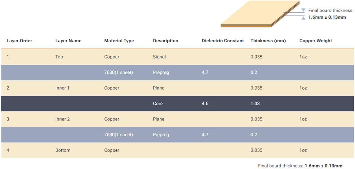
Example standard stackup from Worthington Assembly/CircuitHub.
Aside from this important data, that is about the only information a standard stack-up will contain. There is a lot of information lacking in a standard PCB stack-up, particularly when the board needs to be deployed in a more specialized application. A designer who does not control the stack-up design portion of a project will be at the mercy of the PCB fabrication house.
What's Missing from the Standard PCB Stack-Up?
Let's get a little more granular: What specifically is missing from a standard stack-up? The list below is not universally true, but it is common to see the following list of items missing from a standard PCB stack-up:
- Commercial product name and datasheet
- IPC 4101/4103 slash sheet conformance
- Reliability metrics, such as breakdown voltages and temperature
- Available glass weave styles
- Dielectric constant and/or loss tangent stability constants or curves
- Type of curing agent in the dielectric
- Type of copper foil (electro-deposited, rolled annealed, etc.)
Some fabrication companies do a better job than others of providing multiple stack-up options and more information to help designers select an appropriate standard stack-up. For example, JLCPCB is a popular option among hobbyists and experienced designers who are looking for a low-cost, quick-turn option for PCB fabrication. They provide multiple standard stack-up options for different layer counts and Tg values. These options contain different weave styles, layer thicknesses, and copper weights.

Example standard stackup from JLCPCB.
The other piece of information not provided in a standard stack-up is the trace size required for a specific impedance value. Anyone who is new to high-speed design will quickly learn why impedance targets are important. If the stack-up selection has dielectrics that are too thick, or the designer routes on the wrong layer, some redesign will be needed to ensure the target impedance is hit. This is one of many aspects that drives companies to outsource their design tasks to a PCB design firm.
The Verdict: Should You Use a Standard Stack-Up?
If the design is basic enough that it does not have major reliability concerns, electromagnetic performance requirements, thermal requirements, or specialty builds such as heavy copper, then a standard stack-up is a good option. For what we do, if we are designing a digital PCB that does not have impedance requirements, then we will likely use a standard stack-up unless there are material-related reliability concerns. In the case I just mentioned, the layer thicknesses can become important for EMI and crosstalk reasons, but working with your manufacturing partners and keeping a catalog of their standard stack-up options gives the flexibility needed to meet these requirements.
For a high-speed design or an RF design, particularly where controlled impedance testing is required, the design firm should specify the impedance target and the corresponding trace width on the layers requiring controlled impedance. This is a best practice both for controlled dielectric and controlled impedance PCB stackup design approaches.
An example stackup table we have used on a past project is shown below. This stackup takes a controlled dielectric approach, where the fabrication house is required to mix and match material thicknesses to hit the impedance/width targets listed in the table.

Stackup table for a high-speed PCB.
In other cases, such as when an HDI build is needed, but there is no impedance requirement, a standard stack-up could still be a viable option, but it now depends on the manufacturing process and layer thickness being used in the PCB. For example, I have never qualified a standard stack-up for use in an HDI PCB with laser-drilled microvias, but some standard stack-ups might be usable with mechanically drilled blind/buried vias. Obviously, there is a lot of information to track just when designing a stack-up, which is why it is important to work with a qualified contract engineering firm to build a PCB that can be manufactured at scale.
Whether you're designing high-speed PCBs for mil-aero embedded systems or a complex RF product, you should work with a design and development firm that can ensure your product will be reliable and manufacturable at scale. NWES helps aerospace OEMs, defense primes, and private companies in multiple industries design modern PCBs and create cutting-edge embedded technology, including power systems for high reliability applications and precision control systems. We've also partnered directly with EDA companies and advanced ITAR-compliant PCB manufacturers, and we'll make sure your design is fully manufacturable at scale. Contact NWES for a consultation.
Ready to start your next design project?
Our Clients and Partners


