Guide to No-Clean Flux in PCB Assembly
By A Mughees • Apr 26, 2024Learn about no-clean fluxes and the possible reliability problems they pose in PCB assembly and soldering processes.
Once a PCB is fabricated, the next step is to mount electronic components in a standard PCB assembly process. The PCB assembly process includes a series of procedures that must be followed in the correct order for the final product to function as intended. PCB assembly is the final step in PCB manufacturing that produces a functional electronic assembly that is incorporated into a new product.

Modern electronic devices rely on printed circuit boards (PCBs) as their core building blocks. Assuming the PCB fabrication process was executed correctly, the PCB assembly process is where the true quality of a product will be created and proven. PCB design centers around placing a bare board into the standard assembly process at any level of scale, and expert designers make it their mission to understand the standard processing steps and limitations.
The PCB assembly process involves mounting and soldering components in three possible process steps:
Most modern boards intended for commercial products and advanced technology will be assembled with both surface-mount and through-hole components (hybrid assembly). Most designs will use surface-mount components as they also tend to be smaller, while the larger components like connectors or mechanical parts are still through-hole components.

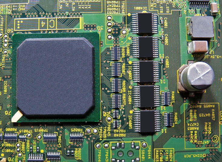
Advanced electronics do not predominantly use through-hole technology for the major components. However, there are many components that are not central to digital or analog processing that are placed as through-hole components. In this assembly process, the component leads are inserted into pre-drilled holes in the PCB. The leads are then soldered on the opposite side of the circuit board. Through-hole components are typically the bulkiest components on a PCB; some example components include transformers, pin headers, and larger power transistors.
The smallest components used in modern microelectronics are surface-mount devices. These components are directly soldered onto the PCB and they do not require drilled holes for mounting. Note that some connectors will have both drilled hole leads for mechanical stability, as well as SMD pads for surface-mounted connectors. Because drilled holes are not required for these components, the PCB fabrication cost could be reduced in simpler boards and production throughput can be accelerated. Component placement can be almost ten times faster than a typical through-hole placement process, and these components can be placed with far higher levels of component density compared to through-hole components.
It is common to see PCBAs with a combination of surface-mount and through-hole components. When providing a circuit board to a manufacturer for quote, the assembler will need to know if the board will use both through-hole and surface mount components. The issue is that mixing components can add additional soldering cycles because the two types of components require different soldering processes. This is discussed in more detail below.
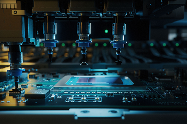
PCB assembly is a guided, step-by-step process. The first step in the process is stenciling, where solder paste is applied to the sections of the board where components will be mounted. Solder paste is made up of microscopic metal balls and a substance called flux. Solder paste stenciling is like screen-printing; solder paste is applied to the bare PCB using a thin stainless steel stencil. A mechanical fixture holds the stencil and the PCB in place while solder paste is distributed over the stencil. The paste is viscous and will remain in the specified areas of the bare PCB after the stencil and applicator are removed.

Component placement is automated using a pick-and-place machine. In the case of through-hole technology, a technician can manually place some components that may be too large for some pick-and-place machines, although at high volume the entire process is generally automated. Fast, accurate, error-free placement with automatic component mounting requires precise numerical data generated from the ECAD data for a design. The pick-and-place file contains each component's X and Y coordinates; this file is generated from CAD software and it is used to program a pick-and-place machine.

Components on the PCB are secured using three possible soldering processes: wave soldering, reflow soldering, and selective soldering. Most boards will only require wave soldering and reflow soldering. Hand soldering is generally not performed in high-volume assembly operations unless rework is being performed.
Wave soldering can be used in both surface mount and through-hole assembly processes, although this will generally be used for through-hole soldering. PCB with all mounted components is moved into a solder line and a hot wave of liquid solder is pulled over the PCB. The solder sticks to the metal portions of the board that aren't covered by solder mask. As the solder cools, it securely fastens component pins to the PCB. Compared to manual soldering, this technique is significantly more efficient and can produce higher quality assemblies.

Reflow soldering is the standard process used for surface-mount assembly. Double-sided boards will pass through two reflow soldering cycles. When used with a hybrid assembly process, this leads to a total of at least three solder cycles (1 wave, 2 reflow, rework cycles) required to fully assemble the PCB. This is an important point to note as some industries require the total number of solder cycles to be limited.
Reflow soldering is completed by placing the components with a pick-and-place machine, and the board is passed into a reflow oven held near 250 Celsius. The oven heats up the solder paste and causes it to harden into a metal joint on the exposed component pins and pads on the PCB.

After the soldering processes are completed, the assembled PCB must be thoroughly cleaned after assembly. This can involve use of deionized water or other cleaning agents to remove any residues from the surface of the PCB, particularly removal of flux residues. After being washed, PCBs are dried with compressed air and the assembled boards are sent for inspection.
To make sure that the assembled PCB is in proper working order, the PCB will be inspected with some automated tests. High-volume production will involve further quality assessments to ensure the overall process is producing defects at acceptably low rates. After inspection, some boards may be further qualified with in-circuit testing, which will involve powering up the board and probing specific points on the PCBA.
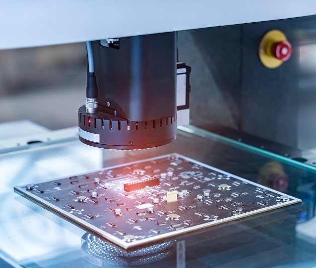
Visual inspection is performed with automated optical inspection (AOI). This vision system uses high-resolution cameras that can be positioned at various angles to visually inspect the surface layers of the PCBA. The goal in this inspection step is to identify assembly defects related to component placement and soldering. These include component alignment, solder joint quality, and any lifting of components during cooling. Large batches of PCBs can be processed quickly with an AOI system.
For single or double-sized PCBs, AOI will be a comprehensive inspection tool, but it cannot be used to examine inner layers on a multi-layer PCB. Instead, multilayer PCBs can be inspected using an X-ray imaging machine. Experienced technicians can inspect these X-ray images visually, although newer systems can automate the inspection process through some image processing steps. When a defect is found in the X-ray image, it is then flagged for further inspection by a human technician. X-ray systems are also commonly used to inspect BGAs for assembly defects, such as creation of shorts or opens, as well as alignment of the BGA on its pads.

Testing processes for a completed PCBA can vary, depending on the needs of the end product and its required level of reliability. The testing processes used to qualify PCBAs can extend beyond in-circuit testing to include mechanical testing, accelerated life testing, and stress tests like thermal and mechanical shocks. These tests go beyond defect detection and basic functionality checks to determine the long-term reliability of the end product. Depending on the standards that apply to your assembly, different testing regimes may be needed and an industry-focused EMS company should be consulted to develop a test plan.
Learn about no-clean fluxes and the possible reliability problems they pose in PCB assembly and soldering processes.

Learn about contract manufacturers, turnkey services, and self-managed production in low volume PCB manufacturing.
Learn more about turnkey PCB manufacturing services and turnkey PCB assembly services for your next electronics prototype or full-scale manufacturing run.


