
When to Use Z-Parameters for Signal and Power Integrity
By ZM Peterson • Aug 7, 2020Every so often, I get a great question from another PCB or IC designer looking for advice on everything from simulation to layout. Here's a great question that I received through SILists, which is a thriving community of signal integrity experts. This particular question is about PDN simulation, but this is intimately related to signal integrity. Here’s the question:
I wanted to know for Package/PCB PDN models for Core PDN's is the typical recommendation to use RLC models (lumped/distributed) or S-parameter models. Any tradeoffs or factors to consider and which is more accurate?. The context for the question is sometimes I see S-parameter PDN models to be inaccurate depending on the tools used.
The answer here is quite interesting and depends on a number of factors. The model used to describe a PDN cannot be automatically extended to other systems, such as transmission lines or any other electrically long distributed network. Therefore, the model used to best describe a PDN conceptually and mathematically should be chosen carefully. Full-wave field solvers are like the nuclear option, but the best option conceptually and mathematically is to use Z-parameters.
What are Z-parameters?
To answer the above question, what is really needed are the PDN's Z-parameters, which will show the self-impedance and transfer impedance for different ports/groups of ports in the PDN. Most SI engineers do not talk about Z parameters unless they’re using some field solver like Ansys SIWave, or unless they are talking about differential impedance. Power integrity engineers should be familiar with Z-parameters for describing the impedance of a PDN. These parameters define the self-impedance and transfer impedances of a multi-port PDN. This is summarized in a Z-parameter matrix, as defined below:
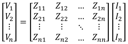
The Z-parameter matrix can then be used to relate a transient current draw at one port to the PDN voltage ripple seen at a different port. Just like S-parameters, Z-parameters obey reciprocity as long as the geometry of the PDN is symmetry (i.e., reciprocal), although in real PCBs and ICs this is almost never the case. In effect, the Z-parameters are like a multiport transfer function for transforming a transient voltage into a transient current. In the above matrix definition, it’s easiest to understand what’s going on by considering a PDN with two output ports (1 and 2). The Z-parameters tell you that the voltage ripple seen at port 1 (V1) depends on the transient current being drawn into ports 1 through n (I1 and In, respectively). This calculation of the voltage ripple in the time domain uses an inverse Fourier transform as shown below:

My opinion is you should use the Z-parameters to calculate the power bus ripple from the transient current draw into single/multiple ports in the frequency domain and then convert these results back to the time-domain to get the peak-to-peak or RMS ripple and compare to your specs. In the frequency domain, the Z-parameters also show you the resonances/anti-resonances in the PDN’s impedance spectrum. Finally, if needed, you can convert the Z-parameters to the PDN’s S-parameters and, finally, to a transfer function.
Wideband S-parameter models are fine, but I personally hate using S-parameters for everything because they get so overgeneralized. For example, you’ll find S-parameters appropriately discussed for transmission lines, antennas, filters/matching networks, or other electrically long structures. These uses are appropriate, but I have never found the conceptual explanation for S-parameters satisfying when applied to a PDN. If you can extract an S-parameter model for the PDN, then you can create a transfer function for a SISO PDN. For a real multiport PDN (SIMO or MIMO system), you need a broadband transfer function matrix, and then you basically know everything about the PDN. If you're in the Laplace domain, you can look at poles in the transfer function to see the transient impulse response and resonances.
What About Circuit Models?
The alternative class of models for describing electromagnetic behavior in a PDN, transmission line, or other systems is circuit models. These are normally LTI systems (linear time-invariant) as these show how the system behaves as a set of equivalent RLC networks; this is applicable when signal propagation is fast compared to the overall length of the network (i.e., electrically short networks). In cases where the network is electrically long and we need to consider signal propagation, a distributed element model can be used to model the electrical behavior of a system.
RLC Models
RLC models are partially phenomenological; they are a nice way to think about what happens in a real PDN, transmission line, or any other system that is electrically distributed in space and includes discrete components. This doesn’t mean RLC models are necessarily "bad" or that they shouldn’t be used. A PDN is basically an LTI system, and many PDNs are small enough to be considered electrically short, so they can be described accurately using RLC models.

The capacitor models in this decoupling network (shown in Cadence OrCAD) include parasitics (ESL and ESR). The equivalent circuit for each capacitor is modeled as an RLC circuit.
There are certainly parasitics that live in the PDN just due to its geometry, and the behavior of signals in the presence of these parasitics can be described in the language of RLC circuits. About the only parasitics you can accurately include as equivalent circuit elements in an RLC model is the plane capacitance for a uniform plane pair with simple geometry, input capacitances on integrated circuits, bond-wire inductance, and any other parasitics that might be described in component datasheets. If you have direct measurements of all these, that certainly helps create an accurate model. Note that this might only be true for a SISO system.
Lumped Element vs. Distributed Element Models
Distributed element circuits provide a bridge between a real PDN (either digital or analog), transmission line, or other distributed elements in a real PCB or IC. Modeling distributed element systems properly requires placing repeated circuit blocks, where each circuit block represents a per-unit-length set of parasitics in the system. The accuracy of these models depends on the number of distributed networks placed in the circuit; it's not uncommon to see 20 or more LC networks placed in a distributed element simulation for a transmission line. One should note that the accuracy of a distributed element model depends on the number of distributed elements included in the simulation, as well as the delay defined between each element. In general, the accuracy is greater when more distributed elements are included in the model.
Contrast this with a lumped element model, where distributed elements are collapsed into individual circuit networks. This is by far the simplest type of model for understanding the time-dependent behavior of propagating signals. A lumped element model basically has the same meaning as any basic circuit diagram; it shows the arrangement of electronic components, so it facilitates an analysis of voltage and current throughout the circuit. However, these models don’t consider the interaction between circuit elements and propagating signals because they do not use per-unit-length circuit elements.
At NWES, we always aim to provide our clients with the most advanced design and analysis services. We help electronics companies design modern PCBs and create cutting-edge technology, and we can aid design teams with advanced analysis, including determining Z-parameters for electrical systems. We've also partnered directly with EDA companies and advanced PCB manufacturers, and we'll make sure your next layout is fully manufacturable at scale. Contact NWES for a consultation.
Ready to start your next design project?
Our Clients and Partners


