
Understanding Characteristic Impedance in Your Circuits and PCBs
By ZM Peterson • Aug 24, 2021Every circuit you design in your system will have a characteristic impedance value. For simple circuits, the term "characteristic impedance" can refer to a circuit’s impedance as calculated from equivalent circuit rules or Ohm’s law. For more complex elements, like structures supporting wave propagation (transmission lines, waveguides, antennas), characteristic impedance is more complex and must be determined from the electromagnetic fields in the system.
Another important consideration is the input impedance, which is the impedance seen by traveling signals as they enter the input ports of a network. This might be equal to the characteristic impedance in some conditions, but this is typically not the case for most DUTs. It is definitely a design goal for transmission lines, which need to support wave propagation without reflections at interfaces by enforcing impedance matching between the line’s characteristic impedance, input impedance, and load impedance. To see how to properly approach input impedance and characteristic impedance in a real PCB, we’ll look at the exact definition of characteristic impedance in a design and how it should be used in analysis.
Definition of Characteristic Impedance
The most general definition of characteristic impedance refers to the impedance of a circuit network or component that is measured in isolation, meaning there are no sources or loads connected. More specifically, this refers to the transmission line characteristic impedance, which can be a complicated function of the following:
- Line geometry: This includes the electrical length and the cross section; both affect the electromagnetic field emanating around the transmission line
- Substrate material (PCB laminate): The substrate material will have dispersion in its dielectric constant, and this will cause the impedance to vary as a function of frequency
- Copper roughness: Roughness on the line; electrodeposited conductors will have rough surfaces, which increases the skin effect and the total impedance
- Nearby conductors Nearby conductors influence the parasitic capacitance and inductance, which will modify the impedance of circuit elements or a transmission line
For a more thorough discussion on characteristic impedance formula and how it can be used for modeling real transmission lines, take a look at my 202 IEEE EPEPS presentation.
Similar statements can be made for a waveguide, arbitrary circuit network, or any other device. However, we don’t use the term "characteristic impedance" to describe the impedance of these elements. For waveguides, we use "wave impedance," while for circuit networks we use "equivalent impedance" or some other term. However, the important quantity that determines circuit behavior in high-speed/high-frequency systems is not the characteristic impedance (or any other impedance term), it is the input impedance into the network.
Input Impedance vs. Characteristic Impedance
When I was a new designer, it was difficult for me to see exactly what the input impedance of a cascaded network was and why this would matter for predicting the response of a transmission line. To see this, it helps to look at a basic circuit and how the equivalent impedance changes when the circuit is connected to a load. Then, the same idea can be applied to any other element in your system, such as a transmission line or waveguide.
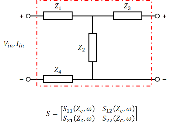
Consider the network below; the output from this network is taken across the 2nd and 3rd impedances. The equivalent impedance measured across the inputs on the left side, is just the sum of Z1, Z2, and Z4 (this is due to the open circuit from the low side of Z3 to the negative terminal). This is the input impedance seen in this network.
Now let’s suppose that we connect a load impedance across the output, and then we measure the impedance across the input ports. Obviously, the equivalent impedance will be different because the circuit is now different. If we measure the impedance across the inputs, we are now measuring a new input impedance. Again, this equivalent impedance measured from the left side is an input impedance, but it is not the same impedance we had before the load Z5 was connected. In fact, the equivalent impedances in each situation will only be equal when the new load impedance is infinite.
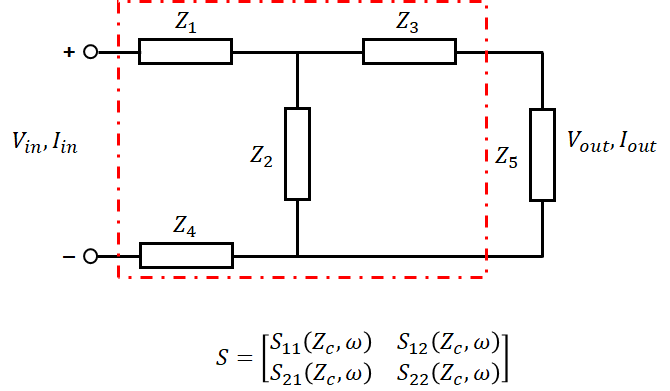
Adding a load component modifies the equivalent measured impedance and the input impedance. If this were a transmission line, we might have a situation where the load also modifies the input impedance, depending on the length of the transmission line.
This should illustrate the importance of input impedance; it determines how an electrical signal interacts with a circuit network, including whether a signal reflects or produces artifacts like ringing. This is also the reason that circuit networks, transmission lines, and arbitrary DUTs are represented with network parameters, transfer functions, input impedance values, and other quantities for cascaded networks. These elements have an equivalent impedance or characteristic impedance when examined in isolation, and that impedance generally appears somewhere in the network parameters (for example, transmission line impedance appears in ABCD parameters and S-parameters). However, equivalent impedance and characteristic impedance do not tell the whole story, and designers need to know how to calculate network parameters using these values in order to better understand their designs.
Summary
To close, if you know how the impedances of a circuit or DUT make up an equivalent impedance, and you know the load network/component to which it is connected, then you can predict how a cascaded network will respond to an arbitrary input. The same idea applies to transmission line characteristic impedance. The important point here is that the exact impedance that affects a system’s electrical behavior is not just its equivalent impedance or characteristic impedance; the load and source impedances matter as well as these will determine an input impedance seen at the input to the network.
The simplest method for predicting the response of an electrical system to an input waveform to insert the input stimulus into the circuit’s governing differential equation in order to predict the voltage/current seen at the output element. More advanced methods will treat the network and any upstream/downstream elements as a cascaded network and use the network parameters to predict the response, similar to a transfer function. In fact, network parameters are transfer functions: as an example, Z-parameters are a transfer function that describes a transformation between voltage and current.
When you’re designing high-speed digital systems or high frequency analog systems, it pays to understand when to focus on characteristic impedance. NWES is an experienced RF PCB design firm that develops advanced IoT platforms, RF power supply designs, data center products, and much more. NWES helps aerospace OEMs, defense primes, and private companies in multiple industries design modern PCBs and create cutting-edge embedded technology. We've also partnered directly with EDA companies and advanced ITAR-compliant PCB manufacturers, and we'll make sure your next high speed digital system is fully manufacturable at scale. Contact NWES for a consultation.
Ready to start your next design project?
Our Clients and Partners


