
The Fundamentals of High Speed Backplane Design
By ZM Peterson • Dec 23, 2020Control panels for aircraft, rugged computing systems deployed on the battlefield, and hot-swappable rack-mount systems all need a high speed backplane design to route signals within the system. Backplanes have an important role in these fields as modular system components. In addition, they need to withstand harsh environments to ensure the entire system can operate as designed.
High speed backplane design can be rather difficult as these boards contain multiple protocols, signal speeds, components, and connectors. There are tight mechanical constraints involved as well as exacting electrical constraints, and these boards are among the most involved projects many designers will face. If you’re looking to a high speed backplane design, keep reading to learn more about the important design requirements and how we approach these designs.
High Speed Backplane Design Requirements
Backplanes can come in a variety of form factors, carry a range of low speed and high speed signals, and have multiple power requirements. Designers working on high speed backplanes need to consider the following aspects of system construction before beginning the mechanical design and PCB layout:
- Standards. Industry groups have defined the VITA standards, OpenVPX standards (based on VITA), PICMG, Industry Standard Architecture (ISA), and others to ensure interoperability.
- Form factor. Backplanes have standard form factors to accommodate products from multiple vendors.Two common form factors for military and aerospace systems are 3U and 6U Eurocard, PCI Mezzanine (PCM), and XMC Mezzanine (PMC with high-speed serial fabric interconnect).
- Stackup and substrate material. The PCB stackup and substrate should accommodate the required net count and board thickness. In addition, the substrate material should have low losses to accommodate long links between connectors on the backplane.
- Pinout. The pinout used in bus connectors will determine the designer’s routing style and overall ease of routing. It will also partially determine layer count as the wrong pinout will make routing rather difficult, which will require more layers.
- Loss budgets. The total allowed loss along a link will determine the number of allowed layer transitions, which substrate is appropriate, and how connectors are arranged. Loss budget will also determine the appropriate pinout (see above).
- Power requirements. Some backplanes (principally those that connect to a power supply) can carry dozens of amps of current, and the stackup/plane arrangement should be designed to accommodate the required voltage and current.
Connectors and Routing
Backplane design is all about selecting, arranging, and routing connectors in a board. The connector needs to accommodate a particular daughterboard pinout and width, which is then standardized across the entire backplane. In high speed backplane design, routing between connectors requires paying attention to loss, skew, and impedance matching within the system. S-parameter simulations are often used for design verification before prototyping to ensure the board will obey loss budgets. Backplane traces are long enough to require controlled impedance for all moderate to high speed signals.
Regarding pinout, this is quite an important point in high speed backplane design as it will determine the appropriate routing style used in the board. Routing used in the backplane for high speed differential channels requires appropriate spacing between traces on the same layer to suppress crosstalk, but the wrong pinout can create new signal integrity problems in a backplane at the connector and during routing. As an example, the pinout below uses interleaved grounding on the pins. The open spaces between pairs of grounded pins is where signals can connect on one layer. Traces can be routed between rows of pins to make connections, which will provide the required isolation between high speed traces and connector pins.
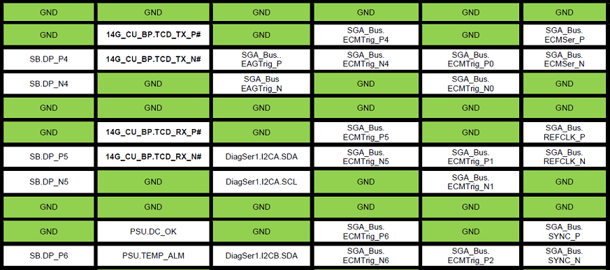
Example pinout in a high speed backplane design. This pinout uses interleaved ground pins to provide isolation between traces reaching the connector.
Aside from routing and form factor, there is the matter of power requirements. We’ve designed OpenVPX backplanes with external power supplies that carry up to 100 A current and at multiple voltages throughout the board. Multiple planes need to be used and a sectioning strategy is often used to separate the main portion of the power polygons from high speed routing regions. If you’re using a high layer count board (e.g., 18 to 24 layers), you’ll have multiple power planes on alternating layers separated by ground. There will inevitably be some layers that are entirely covered in ground pour to provide shielding between layers with high speed signals. The image below shows a partial cross section of a high speed backplane that shows a sectioning strategy one can use for these backplanes.

This sectioning strategy separates high speed differential regions from the main power planes on the same layer, and multiple layers are separated by ground planes.
What’s Next for Rugged High Speed Backplanes
Today’s high speed backplane designs are pushing the limits of copper interconnects. At long link lengths, losses on copper interconnects are dominated by insertion losses, and loss at higher frequencies are approaching the limits of what copper can handle. These limits are imposed in part by copper roughness, as well as losses at connectors and via transitions in a backplane. For this reason, 56G and faster backplanes are increasingly using aperture-based designs with optical fiber to overcome dispersion and losses that accumulate in very long links on high speed backplanes. Broadband design is also a critical consideration for impedance matching and ensuring low loss throughout the signal bandwidth in your backplane.
If your company is pushing the limits of high speed backplane design, it pays to work with an experienced aerospace and defense electronics design firm. NWES helps aerospace OEMs and defense primes design modern PCBs and create cutting-edge embedded technology. We've also partnered directly with EDA companies and advanced ITAR-compliant PCB manufacturers, and we'll make sure your next high speed backplane is fully manufacturable at scale. Contact NWES for a consultation.
Ready to start your next design project?
Our Clients and Partners


