
BGA Escape Routing with Impedance Control in HDI PCBs
By ZM Peterson • Jun 25, 2020When you’re working with HDI PCBs, you’ll most likely be using multiple BGA components. High pin count BGAs need an escape routing strategy to get traces in and out of the bottom of the component. BGA escape routing can be difficult in some situations where controlled impedance needs to be maintained, as is often the case with high pin count FPGAs and other high speed components.
When planning your board, the BGA escape routing technique you need to use will depend primarily on the BGA pitch, which then determines the allowed trace width you can place between solder balls. The limits of your manufacturer, your layer stack, and your required impedance will also dictate how thin you can make your traces. Here’s what you need to consider when selecting a BGA escape routing strategy for your next high speed HDI PCB.
BGA Escape Routing Styles
For fine-pitch BGAs on moderate layer counts, a BGA escape routing strategy begins with neck-down as a trace is routed into/out of the BGA. For the first row of solder pads in the board, the exterior traces can be routed directly onto the pads. For the second row of solder pads on the BGA, the width of the trace is slightly reduced so that it can fit between the first row of pads. For the remaining rows, you’ll need to route through an interior layer to reach the interior pads. In general, you can route into 2 rows per signal layer while maintaining controlled impedance and crosstalk limits.
What happens beyond the first row of pins depends on your BGA pitch, your required trace width, and desired microvia size. Perhaps the most common BGA escape routing and fanout strategy is dog bone fanout, as shown in the image below. This fanout style requires placing a via in a pad, which is placed a short distance away from a solder pad. These vias do not need to be filled plated over as the component is not being soldered directly to the pad with the via. Dog bone fanout is appropriate for 1 mm BGAs and possibly 0.8 mm BGAs.
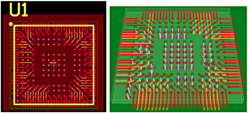
Dog bone fanout is an easy BGA escape routing strategy that is useful for coarser pitch BGAs in HDI PCBs.
Once your pitch gets down to 0.5 mm (~20 mils) or lower, you’re better off using microvia-in-pad for your escape routing strategy. Rather than route a short trace off to the side of a pad, a microvia is placed directly in the solder pad. The microvia is then filled with a conductive epoxy and plated over with copper to prevent solder from wicking to the back of the board. Designing with microvias brings its own challenges (see below).
Using Microvias for BGA Escape Routing
Once your pad size (including annular ring) becomes small enough for a fine-pitch BGA, you’ll need to use microvias for BGA escape routing into the inner layers. The qualities that distinguishes a microvia from a regular via are as follows:
- Via depth. Vias should only span a single layer or, at most, two layers. For very high layer counts on standard thickness PCBs, the via could conceivably extend more layers, although this creates extra fabrication steps. You’re better off using stacked blind and buried vias that span a single layer.
- Via aspect ratio Microvia aspect ratios (length divided by diameter) should not exceed ~2. As an example, suppose we have a 32 layer standard thickness board. The layer thickness (assuming an equivalent 2-layer core) would be ~2 mil, so the diameter should be no smaller than 1 mil. At high layer count, your microvia aspect ratio will be ~1.
Microvias can only be reliably mechanically drilled down to ~8 mils, although the drilling costs per hole at this size can exceed the costs of laser drilling due to frequent drill fractures. Throughput is also lower with mechanical vias than with laser-drilled vias as mechanically drilling needs to be done very slowly to prevent bit fracture. Therefore, you will start to see an overall per-board cost reduction once you start using laser drilling.
For a 0.8 mm pitch BGA (~30 mil pitch), the trace width will need to be ~10 mils or less to enable dog-bone fanout, and your microvia will need to be even smaller (probably ~6 mils). For finer-pitch BGAs (0.5 mm pitch), you’ll likely need to use filled and plated microvia-in-pad to route into the inner layers with 7 mil or 8 mil traces to allow sufficient clearance to nearby pads. No matter which style you use, you can arrange your microvias as stacked or staggered to provide the needed routing density. Pay attention to the IPC 6012 (Rev. D) standards to ensure your microvias and the surrounding annular rings are sized with maximum reliability in mind. Note that BGA pitch can get down to 0.3 mm in some cases, highlighting the importance of microvia-in-pad in BGA escape routing.

Left: staggered microvias are displaced laterally. Right: stacked microvias are placed on top of each other.
Fanout Trace Width and Length: Does Controlled Impedance Matter?
When working with high speed ICs, impedance almost always matters. The relation between fanout routing and impedance control comes into play when we consider the length of a fanout section leading to a longer trace, which then connects to a receiver. The BGA fanout portion will have its own impedance due to the trace length (if present) and parasitic capacitance/inductance of the via.
First, look at the signal bandwidth to see if the impedance of the trace will be noticed by the signal. If the length of the trace is much shorter than the wavelength corresponding to the high-end of the bandwidth (knee frequency for 2-level digital signals), the trace portion of the BGA fanout can be ignored. The best option is to calculate the input impedance of the network formed by the fanout/downstream traces (after neck-down) and the load impedance, which will be a function of the fanout trace length. A decent estimate is to use a 10% limit on the critical length for the signal wavelength. For a digital signal where we approximate a 20 GHz knee frequency, a conservative 10% limit would give a critical length of 0.73 mm (stripline in an FR4 substrate). This means larger ICs, like FPGAs with very high pin count, will require an impedance matched fanout, both for single-ended traces and differential pairs.
Another concern is the inductance of the via, parasitic capacitance between the package/board and land pad, and the pin inductance in the IC. These elements combine to form a low pass T filter (see the circuit diagram below). Here, if you set the via inductance to be equal to the pin inductance, the 3 dB cutoff frequency will simply be the standard value you’d calculate from an LC tank circuit. This equivalent T filter circuit acts like an impedance matching circuit, which modifies the output impedance of the driver IC.

Equivalent T filter circuit for the component pin inductance, via inductance, and substrate/package capacitance on a BGA when routing to the inner layers.
Unfortunately, it's quite difficult to impedance match your fanout without also accurately determining the impedance of the via section that connects your fanout trace to the internal trace. Most designers will just ignore this, which is fine as long as the via section is short and directly traverses a small number of layers. When you're traversing a small number of layers, the input impedance of the (via + internal trace) portion of the interconnect is dominated by the input impedance of the internal trace, so we don't worry so much about the via. The only downside is in very high speed BGA components, such as a very high speed FPGA, which will then need backdrilling to remove the leftover via stub below the BGA fanout. Once you're wroking with HDI, you'll be using blind/buried vias, and ultimately laser-drilled microvias at very small diamaters (less than 6 mil according to the IPC definition), so the backdrilling issue is avoided and the via inductance will be limited by the thickness of the layers spanned and not the board thickness or backdrilling.
At higher layer counts, the layer thickness and distance to the trace’s reference plane will already be smaller, so the trace width will also need to be smaller to compensate and keep the impedance at a desired value. You also need to consider coupling between traces if you’re using differential pairs. The right set of design tools, such as PCB design software with an integrated field solver, can help you design the right trace width for your HDI layer stack to ensure impedance control. You can also take an optimization approach with Wadell’s formulas, as I’ve discussed in another article.
HDI PCB designs can be difficult to master, but the right design firm can create a BGA escape routing strategy for your HDI PCB. At NWES, we design modern PCBs and create cutting-edge technology for major electronics companies. Our projects range from custom computer systems to power electronics and defense/aerospace systems. We've also partnered directly with EDA companies and several advanced PCB manufacturers, and we'll make sure your next layout is fully manufacturable at scale. To see how we can help you with your next design, contact NWES for a consultation.
Ready to start your next design project?
Our Clients and Partners


