
Should You Split Ground Planes in Mixed-Signal PCB Design?
By ZM Peterson • May 2, 2021Probably every designer understands the basic idea behind grounding. A ground reference is needed to provide a consistent 0 V reference throughout an electrical system, including mixed-signal electronics with analog and digital sections. In something like a mixed-signal PCB, the situation can get complicated when there are multiple regulators involved, multiple ground references, and multiple frequencies.
Although mixed-signal PCB design follows a simple concept, it relies on one critical area that relates to signal integrity, power integrity, and EMI: designing a grounding strategy. Many designers are still following 30-year-old design guidelines, which state that a split ground plane should be used in mixed-signal systems. Unfortunately, in today’s modern electronics, outdated design guidelines state that the digital and analog ground plane should be split or sectioned, and this is often implemented incorrectly.
Bad Grounding Creates EMI Problems in Mixed-Signal Systems
We occasionally get client requests to help debug a system that is having EMI problems, causing the design to fail EMC tests. This can be a frustrating experience, especially when you’ve done everything else correctly. The very first place we look when failed EMC tests are a problem, especially due to radiated emissions, is the PCB stackup and the grounding strategy. This is especially problematic in mixed signal systems that may involve a chassis ground, where untracked return paths and differing ground potentials in the system create radiated and conducted EMI.
One recommendation you’ll see for solving a lot of problems in mixed-signal PCB design is to split the ground plane into an analog section and a digital section. Unfortunately, if not implemented correctly (it is almost never implemented correctly), this creates more EMI problems than it solves, leaving the inexperienced designer wondering why they are having noise problems.
- The best grounding strategy for mixed-signal boards with low layer count is to use a single ground plane without any splits, and try to follow return paths for your signals to prevent mixed-signal crosstalk between analog and digital components.
Split Ground Planes
When I refer to a "split ground plane" or "split analog and digital ground planes," I’m talking about one of two types things:
- Two physically disconnected ground regions (analog and digital) on the same layer, meaning the grounded copper regions do not have any electrical connection between them.
- A single copper plane layer, but with some ground cut out from the plane, where the ground cutout separates an analog region from a digital region.

In these examples, we have two common ways many design guidelines will tell you to define ground in mixed-signal PCB design.
I think the ambiguity around sectioning off a ground plane vs. a pair of totally split ground planes leads to the controversy around grounding guidelines in mixed-signal PCB design. Generally, when you intend to refer to the second option above (on the right), everyone assumes you are referring to the first option (on the left). Unfortunately, when trying to implement either option, designers will break some basic rules involved in routing common low-speed and high-speed digital interfaces, or with analog signals, all of which will lead to greater radiated emissions from your PCB.
The first option (on the left) is only appropriate in one corner case, although it ends up being a trivial design. The second option can be justified, but only if the design is routed correctly, and it usually ends up being a trivial design anyways. Again, almost every time I’ve seen this practiced and routed, it’s been done incorrectly and creates a radiated emissions problem that prevents successful EMC testing. Let’s look at these in more detail before we look at the best grounding strategy for your mixed-signal PCB.
Split Ground Planes Interfere With Routing
The reason so many designers fail when using split ground planes in a mixed-signal PCB is simple: they don’t route the board correctly. When you have physically separated ground planes, you should never route over the gap that separates the two planes. This is a basic rule in high-speed PCB design, but it really applies to any digital signal with fast edge rate. Today’s slow-speed digital bus protocols (SPI, I2C, etc) can have edge rates on the order of 10 ns, which is fast enough to cause strong radiated EMI that leads to failed EMC testing.
Whenever I see a failed design involving two totally separated ground regions, it looks like the image below. Because the planes are split, but your components in your mixed signal system need to communicate, you inevitably route over the gap between the planes. This creates your EMI problem. There will be no clear return path, giving an interconnect with huge loop inductance, and thus strong radiated EMI.
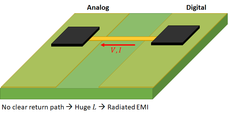
EMI failure in mixed-signal PCB design with separate ground plane regions.
A mixed signal PCB design can still fail when the planes are connected if the designer routes over the split between the two planes. This also creates a return path with large loop inductance, again producing strong radiated EMI. This problem would not occur if routing only occurred over the unsplit copper area. This is exactly why you shouldn't use splits in any ground plane: the second you route over the split, you've created an EMI problem that's worse than the isolation problem you were trying to solve by placing a split in the plane in the first place.
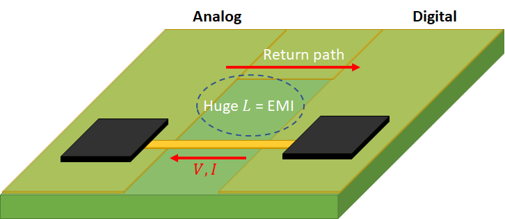
EMI failure in mixed-signal PCB design with connected ground plane regions, but with routing over the gap in the ground plane.
In many cases, a designer will try to bridge the gap with a capacitor, or sometimes with a ferrite bead. Using a capacitor is the least bad solution. I cannot stress enough, don’t try to provide a low impedance return path across split ground planes with a ferrite bead. These components act like bandstop filters, meaning they have a resonance that will radiate strongly if excited with a switching digital signal.
Instead of following decades-old design guidelines with split planes, follow best practices with digital design and use a single, uniform ground plane to support your mixed signal PCB design. If you can follow some basic PCB routing guidelines, you’ll likely be successful with mixed-signal design and prevent interference without using split ground planes.
A Single Ground Plane Makes for Easier Routing
Once you understand how return paths form through displacement current in the PCB ground plane, you’ll suddenly realize that modern digital signaling protocols will quite closely follow their source traces, and splitting ground planes (in both manners shown above) becomes unnecessary. Add to this the copious use of ground pour around lower frequency analog signals and other digital signals, and you have a situation with high analog-to-digital isolation. In this case, you don’t need a physical separation between ground planes to provide electrical isolation; signals will naturally isolate themselves.
Doing this successfully requires following a couple of simple rules:
- Component placement: Group components by function and by circuit block. If a group of components need to connect to each other to provide a specific function, then place them close to each other, don’t route them all over the board.
- Routing: Pay attention to where things are being routed and use some structures to isolate analog and digital signals. Even though signals above a ground plane will follow their source traces, mixed-signal crosstalk can still occur between analog and digital signals.
- Ground plane span: Allow the ground plane to span totally beneath your circuits; don’t do this silliness with placing splits unless you intend to route over copper throughout the board.
If you can follow some basic PCB layout and routing strategies, you won’t need to worry about split planes and the EMI problems they inevitably create.

These components work together to provide a specific function in the system, so place them together to allow tight routing.
The Verdict: Use Solid Ground Planes
At the end of the day, the best mixed-signal PCB design guideline I can give is to use a solid ground plane without any cutouts or gaps. It’s easiest to route, and it helps solve multiple EMI, power integrity, and signal integrity problems that can’t be fully addressed with a split or sectioned ground planes. Doing this correctly requires tracking your return paths in your design, but ironically, it’s actually easier to track return paths for high speed/high frequency signals because they will closely hug traces that carry them. Follow the sectioning strategy, where digital and analog circuit blocks are laid out generally in their own regions of the board, but keep the entire ground plane uniform to the greatest extent possible.
In high layer count PCB with multiple ground and power planes, I often see the split plane guidelines start to crop up again. The design can get much more complicated, and this is especially true when you bring in a chassis ground that might induce common-mode currents in your system. If you want to avoid the complexity and hopefully prevent failed EMC testing, an experienced PCB design company can help.
If your company is pushing the limits of telecom, data center, and aerospace electronics, don't rely on old tricks like using split ground planes in a mixed-signal PCB layout. It pays to work with an experienced electronics design firm. NWES helps private companies, aerospace OEMs, and defense primes design modern PCBs and create cutting-edge embedded technology. We've also partnered directly with EDA companies and advanced ITAR-compliant PCB manufacturers, and we'll make sure your next high speed digital system is fully manufacturable at scale. Contact NWES for a consultation.
Ready to start your next design project?
Our Clients and Partners


