

TEMPEST requirements are often discussed in terms of shielding rooms, filtered penetrations, and installation rules for equipment and cabling. That is where many engineers first encounter the topic, but the real work starts much earlier. If a design contains both sensitive plaintext data and encrypted or otherwise non-sensitive data, then the PCB becomes part of the emissions-control strategy. At that point, red/black separation is not just a system integration problem. It becomes a board partitioning, stackup, layout, return path, and power architecture problem.
In TEMPEST terminology, RED refers to circuits or signals carrying sensitive unencrypted information. BLACK refers to circuits or signals carrying encrypted data, non-sensitive data, or other information that is not treated as exposed plaintext. The goal is simple enough: do not allow RED information to couple into BLACK circuitry or leak out of the product through unintended electromagnetic paths. The problem is that this is rarely solved with a single layout rule or one shielding feature. It requires a deliberate architecture.
Start With a Physical Boundary
The first mistake in mixed-sensitivity designs is treating the RED/BLACK boundary as a documentation label in the schematic rather than a physical rule in the layout. If the domains are only separated logically, the board will usually end up with shared reference regions, mixed return paths, or connectors that force the two domains back together. The design may still function, but it will be much harder to control compromising emissions.
A usable red/black partition should appear in three places at the same time:
- In the system block diagram
- In the schematic hierarchy
- In the physical board floorplan
If those three views do not match, the layout usually devolves into a normal mixed-signal board with a few keepouts added later. That is not a TEMPEST strategy. A better approach is to place RED and BLACK circuitry in clearly separated regions and define a controlled interface between them. If encryption, digital isolation, optical transfer, or filtering is required, that conversion point should sit directly on the domain boundary rather than buried inside one section of the board.
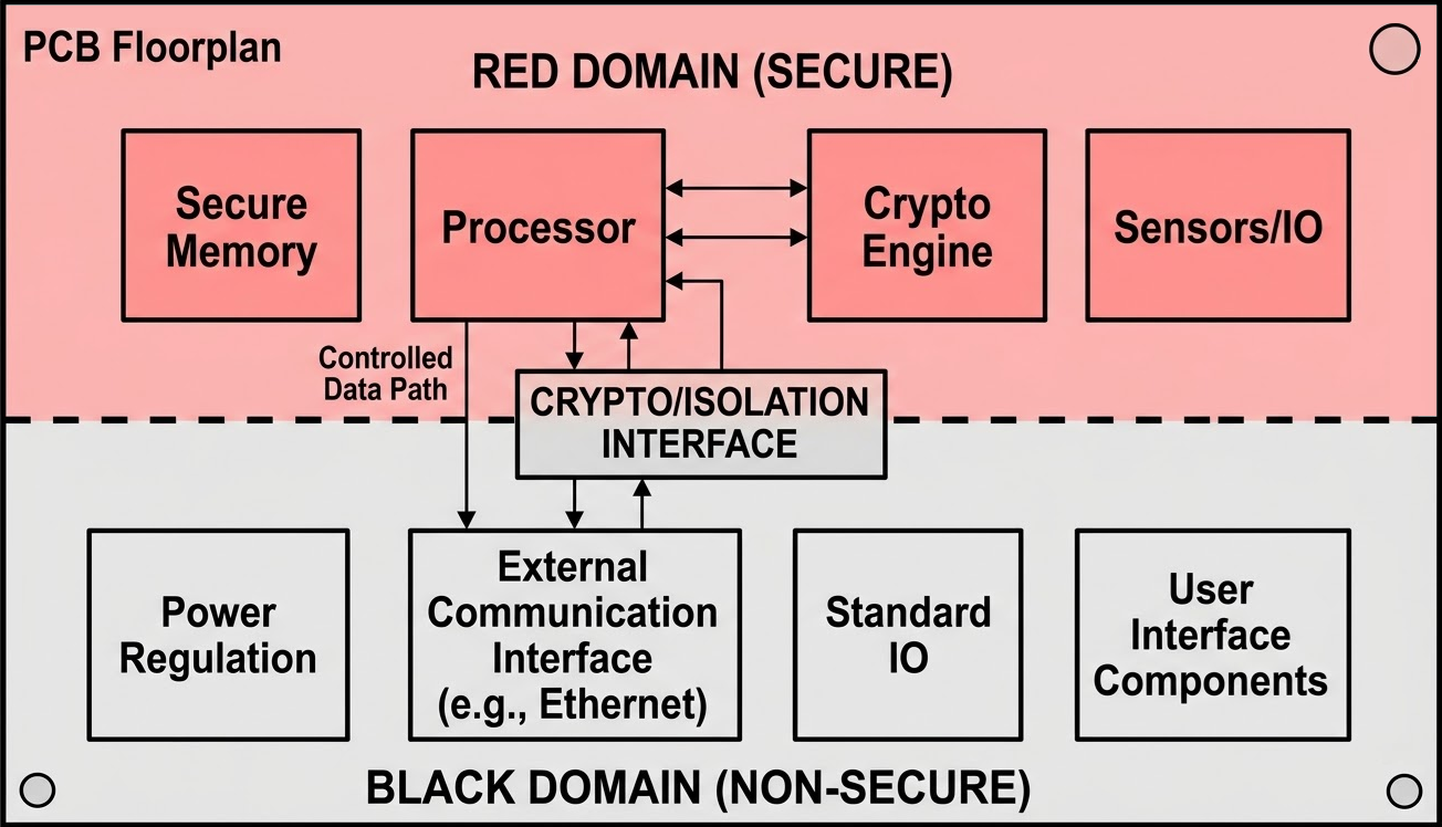
Example PCB floorplan showing RED and BLACK domain partitioning with a controlled interface boundary.
Physical Spacing Is Not the Whole Solution
Physical spacing is the most obvious control because distance reduces both capacitive and inductive coupling. The same reasoning used for cable and raceway separation at the installation level also applies on the PCB. RED and BLACK nets should not be routed in parallel for long distances, and they should not overlap broadside on adjacent layers unless there is a deliberate shielding structure between them.
That said, spacing alone is not enough. A board can have generous clearance between RED and BLACK traces and still create a strong coupling path through shared reference copper, poorly controlled return currents, or common power structures. This is where many designs fall apart. The designer sees physical distance and assumes the problem is solved, while the real coupling path exists somewhere else in the stackup.
Return Path Control Is Usually the Real Problem
In practical PCB design, the dominant issue is often not the signal conductor itself but the path its return current is forced to take. A RED signal only remains well contained when its return current can flow directly under or adjacent to the signal path with minimal loop area. If that return path is interrupted by a split, void, neck-down, connector transition, or poorly managed layer change, the current spreads and the loop grows. Once that happens, the emissions problem gets worse very quickly.
This is why red/black separation is tightly linked to stackup planning. A continuous reference plane can help reduce electric field coupling, but it does not automatically isolate two domains if both domains dump current into the same plane region. The plane may look like a shield in the layout viewer, but electrically it can still be acting as a common transfer medium. That is one of the more annoying realities in this type of work: copper that looks helpful is not always helping.
PCB Structures That Help Enforce Separation
On the board itself, the tools available to the designer are fairly familiar. The difference is that they have to be used as part of a controlled architecture rather than as after-the-fact EMI patches.
Some common structures include:
- Distinct placement regions for RED and BLACK circuitry
- Keepout areas around the domain boundary
- Grounded via fences along sensitive edges
- Shield cans over especially sensitive RED sections
- Guard copper tied into a controlled reference structure
- Layer assignments that avoid broadside RED/BLACK overlap
These features can reduce field coupling and help constrain energy near its source, but they only work when the return path and PDN are also managed correctly. A via fence around a badly partitioned layout is mostly decorative.
Boundary Crossing Should Be Treated Like an Interface
Every RED/BLACK crossing is a risk point, so the number of crossings should be minimized and each crossing should be intentional. This is where isolation devices, optical links, filtered interfaces, transformers, or encryption hardware usually sit. The design objective is to force energy transfer through a known control point and prevent random signal jumps across the partition because placement got inconvenient.
The table below captures the difference between a disciplined boundary treatment and the kind of layout shortcuts that create problems later.
| Design Area | Good Practice | Common Failure Mode |
|---|---|---|
| Domain placement | RED and BLACK circuits occupy distinct board regions | Functional blocks are intermixed for routing convenience |
| Inter-domain signals | Cross only at a controlled boundary interface | Multiple ad hoc crossovers scattered through the layout |
| Reference structure | Return paths are continuous and localized | Shared reference copper allows current spreading |
| Layer usage | Avoid broadside RED/BLACK overlap | RED and BLACK traces overlap on adjacent layers |
| Shielding | Via fences, guard copper, and cans support partitioning | Shield features added without controlling current flow |
Power Domains Can Defeat Signal Isolation
A lot of engineers initially think of red/black separation as a signal routing problem. It is not. The power distribution network can couple noise between domains just as effectively, and in modern digital systems it often becomes the main problem. Fast edge rates and large transient currents can inject wideband noise into shared rails and references, which then reappears in the other domain as conducted or radiated energy.
This is why RED and BLACK sections should usually be treated as separate PDN regions with controlled interconnection. That does not always require completely independent upstream supplies, but it does require deliberate filtering, local regulation where needed, separated decoupling clusters, and careful control over where the domains bond into common structures. If RED and BLACK logic share regulators, planes, or return bottlenecks, then the board has already created a coupling mechanism before the signal routing is even reviewed.
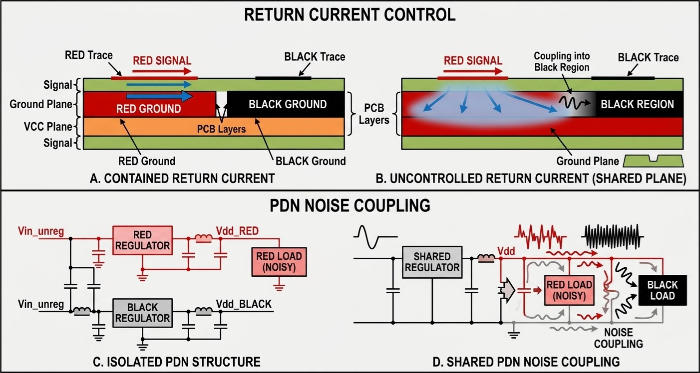
Return current and PDN coupling example showing how shared reference and power structures can defeat RED/BLACK separation.
Connectors and Mechanical Structures
A well-partitioned PCB can still fail once both domains exit through the same connector with poor pin assignment or weak shield termination. RED and BLACK signals should not be casually interleaved at connector interfaces, and cable shield bonding needs to be treated as part of the electromagnetic design. The PCB-to-cable transition is often where a contained field turns into a product-level emissions problem.
Mechanical parts also matter more than many board designers want to admit. Mounting rails, heatsinks, stiffeners, brackets, and other unintended metallic structures can act as coupling surfaces or conductive bridges between domains. In TEMPEST-oriented hardware, those parts are not just mechanical details. They are part of the EM design whether anyone likes it or not.
Red/black separation in PCB design is ultimately about controlling where fields exist, where currents flow, and how energy is allowed to cross boundaries. That requires more than spacing rules and more than a note on the schematic. It requires the RED/BLACK boundary to be embedded in the architecture, reflected in the floorplan, enforced in the stackup, and preserved through the power system, connectors, and enclosure interfaces. Once designers approach it that way, the problem becomes much more manageable and much less dependent on heroic fixes at the end of the project.
Whether you're designing high-speed PCBs for mil-aero embedded systems or a complex RF product, you should work with a design and development firm that can ensure your product will be reliable and manufacturable at scale. NWES helps aerospace OEMs, defense primes, and private companies in multiple industries design modern PCBs and create cutting-edge embedded technology, including power systems for high reliability applications and precision control systems. We've also partnered directly with EDA companies and advanced ITAR-compliant PCB manufacturers, and we'll make sure your design is fully manufacturable at scale. Contact NWES for a consultation.
Ready to start your next design project?
Our Clients and Partners



















