
Low Power PCB Design for IoT and Mobile Devices
By ZM Peterson • Nov 11, 2019The current trend in new IoT devices is packing more capabilities into a smaller form factor, alongside greater processing power, more wireless communication protocols, and greater processing speed/memory.
This trend is pushing more designers to become experts in HDI design, low-EMI stackup design, RF layout and routing, and other formerly advanced areas of PCB design. This is also forcing many design teams to become familiar with embedded software packages, operating systems, UI/UX design, and algorithm design.
No matter which of the above capabilities your next IoT device includes, it will need to be designed to have low power consumption, stable power regulation with near zero power fluctuations, low conducted and radiated EMI, and plenty of sensors/HMI to interface with the real world. Arguably, the most important of these aspects is low power PCB design; if the device can’t operate for more than an hour, then it will never last in the market.
Getting Started with Low Power PCB Design for Mobile and IoT
Low power PCB design is about more than choosing components with power consumption, although this is certainly an important design aspect. Your design should start by considering the power source as this is the most important determinant of usability. Will your device be battery-powered or does it require a wall outlet? If it is battery powered, how long will it need to run before requiring a recharge? This should be the first place to start when selecting hardware for your next IoT/mobile product. Some designers tend to start from the other direction; selecting processing power and memory (RAM and Flash) is important for ensuring any embedded software can run with minimal computation time. This then dictates the power requirements for your device, but this can hinder functionality; in other words, the mobile device you desired to create may not be fully mobile as it requires frequent recharging, an excessively large battery, or it requires constant wall power.
Active devices (MCUs, FPGAs, SoCs/SoMs, and any other IC that processes or manipulates data) should be chosen such that they only provide the required processing capabilities with minimal power consumption. Many MCUs that offer processing power for data-intensive tasks and other SoCs for signal processing and other tasks have a built-in sleep mode. When the component in question enters sleep mode, it effectively shuts down and uses a minimum amount of power as it waits for a wake signal.
Once you do determine your battery size, maximum power consumption, and required supply voltages in various components, you need to select components that provide stable power as the device operates. Providing stable power is an important part of power integrity, although this is intimately related to EMI problems within and outside the product, as well as signal integrity. Solving all of these challenges at once requires making the right board design decisions. This includes stackup design, PDN design, and isolation in your routing and layout. We've addressed PDN design in a number of our other blog posts, so we would like to focus on stackup design, layout, and routing in this post.
Get Your Stackup Right
Your stackup will be a major determinant of power integrity and isolation in your layout. Advanced PCBs for IoT devices will likely use a minimum of 6 layers, but densely-packed boards with high pin count PLDs can easily span a couple dozen layers. You may want to use a flex or rigid-flex board in order to satisfy your form factor requirements. As an example, the newest iPhone uses about two dozen flex boards in order to provide extra room for a larger battery.
No matter how many layers you include in your board, the major challenge in designing your stackup is providing room for stripline routing, and placing your power and ground planes on adjacent layers. This will provide significant decoupling and reduces the number of decoupling capacitors required in your board to ensure power integrity.
The stackup shown in Fig. 1 is useful for a number of reasons. First, even on a standard 1.57 mm board, the adjacent power and ground planes will have significant interplane capacitance, which helps decrease the total equivalent impedance of you PDN. Once a few decoupling capacitors are added for critical components, you’re likely to have very stable power distribution in this board with sufficiently low ringing. If you are working at lower signal levels, you may be better off working with a higher layer count on a thinner board if possible, as this will push your power/ground planes closer together and provide larger interplane capacitance. Second, the arrangement of alternating ground planes and signal layers allows for stripline routing in interior layers. The adjacent ground planes will provide a close return path with low loop inductance, which will provide shielding and help suppress ringing.

Fig. 1: Example 10-layer rigid stackup for ensuring power integrity in low power PCB design in IoT/mobile devices.
Routing between layers is another point to consider, especially as the density of traces and components in your board increases. As more devices reach higher density, HDI design techniques become more attractive. Not much changes on the design side as far as traces are concerned, but fanout techniques for high pin count components and via design change significantly. When you’re designing a fanout strategy, your options are essentially dogbone fanout and via-in-pad. Three possible variants for fanout/escape routing are shown in Fig. 2 below.
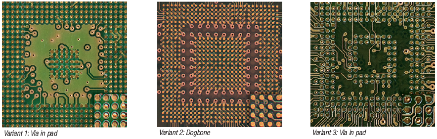
Fig. 2: HDI fanout options for high density BGAs in low power PCB design.
Low Power PCB Design and EMI/EMC
Your next IoT product will likely contain multiple DC-DC converters. Your upstream regulator will need to connect directly to your power source and can be used to drive downstream DC-DC converters. These converters for IoT devices generally run at 100’s of kHz to a few MHz, meaning they can be a problematic source of radiated and conducted EMI. The stackup points mentioned above are important for shielding and suppression of radiated emissions, but making sure switching noise does not interfere with downstream components also requires placing components in the right location.
There is little you can do to combat conducted EMI from switching noise except to use filtration. The output capacitor on a regulator circuit goes a long way towards reducing switching noise. However, your switching regulator also produces radiated EMI that can induce a strong voltage fluctuation in a nearby circuit. Switching regulators/converters that produce a few Amps of current can induce a few Volts worth of noise in a nearby circuit. Vias and circuits with high loop inductance can be problematic points where voltage is induced by a switching regulator.
The most sensitive circuits, antenna elements, analog circuitry, and any other digital signals that run at low level (less than 3.3 V) should be placed farthest from your power conversion circuitry. This will ensure that radiated EMI that does reach these components has decreased in strength by the time it reaches these components, thus it will induce less noise. Another point to consider is where you place your input/output capacitors and output inductor for your converter ICs. These should be placed as close as possible to the converters and should not be routed with vias. The exception is your input/output capacitors; the ground pin on these capacitors should be routed through a via directly back to the adjacent ground plane to reduce loop inductance.
In extreme cases, where you are working with an IoT/mobile device that supplies high current, you should consider using some shielding techniques to reduce radiated EMI between the power section and your antennas, analog circuitry, and any other components that run with low supply voltage. Shielding cans are one option; you can easily house the power regulation section of your board in grounded shielding cans. The other option, which may work best with small form factor flex/rigid-flex boards, is to use via fences and ground pour to isolate different functional blocks. Via fences are normally sized to create an image charge for a specific wavelength. In contrast, ground pour will provide broadband shielding and isolation, but the attenuation this provides will be lower than that provided by a grounded via fence. Some post-layout simulation tools will be useful here for verifying your isolation techniques and ensuring any induced noise does not exceed noise margins in your circuits.

Fig 3: Shielding for IoT/mobile devices for ensuring power/signal integrity.
Low power PCB design is as much about energy conservation as it is about power integrity and stability. If you’re looking for a knowledgable firm that offers cutting-edge PCB design services and technology research services for innovative electronics companies, contact NWES for a consultation.
Ready to start your next design project?
Our Clients and Partners


