ADC Noise Reduction in Your Analog PCB Signal Chain
By ZM Peterson • Oct 24, 2019Your next IoT device, mixed signal system, electro-optical system, or industrial control system will likely take advantage of one or more ADCs. While many MCUs and FPGAs include one or more built-in ADCs, the available resolution may be limited, and you’ll have less flexibility in designing the signal chain in your new product’s analog front-end.
If you are experimenting with a new signal chain design on the road to creating an integrated SoC/SoM, or you are working in an entirely new area, then your sampling rate, input level, and some simple layout choices will affect noise on the output from your ADC. What should you do if the output from your ADC is noisy? There are some strategies for ADC noise reduction, including oversampling, filtration, and reducing board temperature. Here are some strategies you can take when working with an ADC and how you can reduce error in the digital output.
ADC Operating Parameters and Noise
There are some important parameters to consider when choosing the correct ADC for your application. Choosing the ADC with the highest possible resolution is not always the best choice for your system. If you are gathering sensitive AC measurements and you need highly accurate quantification of your results, then you should opt for a higher resolution. You should also opt for higher sampling rate when working at higher frequencies. In contrast, if you are gathering DC measurements and you are converting some DC level with noise to a number using a calibrated scale, your resolution should be similar to the number of measurements in your calibration scale, and you should use a filter on the input of your ADC. The bandwidth of your component is also important as it defines the range of frequencies you can reliably convert to a digital signal.
In general, your sampling rate will need to scale with your signal frequency. Choosing the wrong sampling level can lead to aliasing, and it can fail to suppress noise in the output from your ADC. Understanding how the sampling rate affects the output from your ADC requires considering the presence of noise on the input signal. There are a number of ways to measure and quantify noise, as shown in the equations below.
Resolution and Sampling Rate
The resolution of an ADC is specified in terms of the number of bits, which defines the number of distinct output steps (2^n) the converter can produce. In other words, resolution is the smallest voltage increment corresponding to a step change. In general, the resolution of an ADC decreases as sampling rate increases. Many ADCs are simply run at the Nyquist sampling rate. However, as we will see shortly, oversampling with an ADC is a useful strategy for noise reduction, albeit at the cost of higher power consumption. Sigma-Delta ADCs are one type of ADC that uses much higher sampling rate than the Nyquist rate.
SNR, THD, SINAD, and EOB
Signal-to-noise ratio (SNR) is defined as the ratio of the output signal level to the output noise level. It is usually represented in decibels (dB). Total harmonic distortion (THD) is defined as the ratio of the sum of powers of any harmonic frequency components on the input to the power of the fundamental/desired frequency component. This is calculated in terms of RMS voltage. Note that ADCs are slightly nonlinear and it generates higher order harmonics during conversion. The input can also contain spurious harmonic content (see below), which can pass into the ADC.
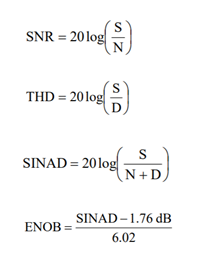
Signal to noise and distortion (SINAD) is a combination of SNR and THD. It is defined as the ratio of the RMS signal amplitude to the RMS value of all other spectral components, including harmonics, but excluding DC. The effective number of bits (ENOB) is the number of bits with which the ADC behaves like a perfect ADC. It is another way of representing SRN, and ENOB can be derived from SINAD.
Noise and Quantization Error
All noise sources on the input signal can produce quantization error. The output from an ADC has discrete steps, meaning every digital step represents a range of analog values. This type of error refers to misclassification of the input signal level due to the discrete distance between different quantized signal levels. For a given RMS noise level, an ADC with higher resolution will have larger RMS quantization error, simply because the distance between different quantized signal levels is smaller.
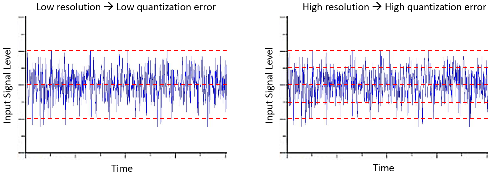
Fig. 1. This image shows how a given RMS noise level on the input of the signal produces quantization here. Here, we have a 10 mV RMS noise level on the input. At any given time, random noise fluctuations will cause some ambiguity in the output from the ADC.
Different noise sources can be easily identified in the frequency domain. What often appears as completely random, uncorrelated noise in the time-domain can arise from a number of discrete frequency components in the input signal. These discrete frequency components can arise from a number of sources, such as harmonics generated from a clock signal, from an analog power amplifier run near saturation, or other nonlinear components in your signal chain.
Obviously, you want to remove these undesired frequency components with filtration, but other sources of noise cannot be so easily removed as they span the entire bandwidth of the filter. 1/f noise, Johnson-Nyquist noise (i.e., thermal noise), and shot noise are continuous, uncorrelated noise sources that require some other method to remove. Although the thermal noise bandwidth is usually on the order of nV per square root of frequency, once the signal is input to an ADC and sampled across the ADC’s bandwidth, you can pass a significant noise signal into the converter, as shown in Fig. 1. This noise can be reduced by oversampling.
ADC Noise Reduction Through Oversampling
Oversampling an input signal is equivalent to averaging, where the input signal level is reduced by the square root of the number of measurements used for averaging. If you oversample an input signal by a factor N, you effectively reduce the input noise level by the same factor. This is because the input noise is spread across a broader bandwidth, which reduces the RMS noise level.
After oversampling, passing the output through a digital bandpass filter with bandwidth equal to the original sampling frequency (normally the Nyquist frequency), removes the excess noise at higher frequency components. Fig. 2 shows how this works in the frequency domain. Note that we are considering the case where spurious harmonics have been removed from the input signal using filtration, leaving behind Johnson-Nyquist noise and other random uncorrelated noise sources.
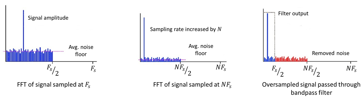
Fig. 2. ADC noise reduction through oversampling.
This oversampling scheme for ADC noise reduction allows you to reduce the impact of noise on quantization error when working with wide bandwidth, high resolution ADCs. As long as the subsequent filter bandwidth is smaller than the ADC input bandwidth, you’ll be able to reduce the noise level within your desired frequency measurement range. If you need a wide bandwidth and you are working over a broad frequency range, then you may be better off working with active bandpass filtration on the input of the ADC. Another option is to use lock-in amplification, where the analog signal is chopped, rectified, and sampled at the chopping frequency.
Beyond the signal processing steps shown above, your PCB layout will influence the susceptibility of your ADC to conducted and radiated EMI, as well as mixed signal crosstalk. Your ADC will need to straddle the analog and digital sections of your ground plane in order to operate properly. Thankfully, ADC suppliers usually provide guidelines in the datasheet, which will help with ADC noise reduction. Signal integrity and power integrity simulation tools are invaluable here as well, as they can help you examine how your system will behave in the presence of different types of noise.
Mixed-signal PCBs will make copious use of ADC/DAC components, and ADC noise reduction is critical for preventing signal problems and incorrect signal processing results. If you’re looking for cutting-edge PCB design services and SEO & thought leadership marketing services, then you need to work with NWES. We're an experienced design firm that specializes in all areas of PCB design. Contact NWES today for a consultation.
Ready to start your next design project?
Our Clients and Partners


