
Using CCD Sensors for Imaging and Spectral Measurements
By ZM Peterson • Sep 18, 2019I originally came from the world of optics, and we routinely used CCD sensors in our optical systems for gathering spatially resolved spectral measurements with microscope systems.
In cameras, CMOS image sensors are extremely useful for monochrome and color imaging, and the choice of which type of sensor to use will be obvious for your system. However, CCD and CMOS sensors are quite different, and each type of sensor will be ideal for different applications.
CMOS vs. CCD Sensors for Imaging
CCD imaging sensors generally provide light detection with lower noise and higher sensitivity. In contrast the way a CMOS sensor converts an optical signal to an electrical signal (using a photodiode) is faster than in CCDs (see the Addressing section below). When used for imaging, CCDs generally provide finer images thanks to the low noise in their output, making them ideal for sensitive spectral measurements or image measurements. In terms of imaging, most CCDs respond slower than comparable CMOS image sensors, which limits their use to imaging applications with low frame rates. High resolution CMOS sensors (i.e., MP cameras) can easily respond faster than a human's persistence of vision.
While CCDs provide higher sensitivity and lower noise figures, they do come with higher costs, simply because they are not produced at the same scale as CMOS sensors. This arises for two reasons. First, CMOS image sensors can be produced using the same process as CMOS-based ICs, making them massively scalable. Second, the market for devices with portable cameras (i.e., smartphones) is massive, while the market for devices that provide sensitive spectral measurements is not. The high frame rates provided by CMOS sensors makes them ideal for use in consumer electronics. There is still plenty of debate on the quality of images produced with CMOS vs. CCD sensors.
A back-side illuminated (BSI) CMOS sensor is similar to a standard CMOS sensor, but it uses a different architecture. In this type of CMOS sensor, the order of the copper conductors and photodiode in a pixel are reversed, allowing each pixel to receive more light and operate in low-light conditions. Some CMOS sensors will include an absorptive film that blocks infrared light from being detected by pixels. If you take an infrared TV remote and point it at your smartphone camera, you'll likely be able to see a purple-ish flash of light in video mode. CMOS sensors for infrared imaging systems will omit this infrared film and will optimize the pixel geometry for capturing infrared light.
Addressing
The frame rate difference between CCD and CMOS sensors are due to the way in which pixels are excited and charge carriers are extracted with the underlying electronics. CCDs use a global exposure technique to excite the entire sensor. Columns of pixels are then shifted across the sensor, and each pixel in a column is read individually as serial data. This is all done using shift registers, as shown below. Here is a link to a study where the imaging process with a CMOS image sensor was examined in SPICE and Matlab; this should provide some context for the imaging process in a CMOS sensor.
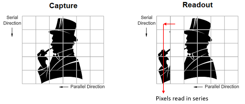
This image shows how data is shifted across a CCD and is read pixel-by-pixel from each column.
Meanwhile, CMOS sensors use row and column addressing to expose each pixel individually. Each pixel contains an integrated amplifier that feeds the excited signal into an ADC (normally integrated on the back side of the sensor). Individual addressing reduces unnecessary shifting between each row/column across the sensor. Furthermore, CMOS components switch very quickly, allowing the signal from a CMOS sensor to be averaged with an off-board processor as desired. These two factors allow a CMOS sensor to operate faster than a CCD with the same number of pixels.
Resolution
While the number of pixels is most often cited as the primary factor that determines resolution in a digital imaging system, this is actually incorrect. The pixel size or pixel pitch (the two terms are basically equivalent) will determine the resolution of your imaging system, and the number of pixels will determine the field of view you can capture in your images. Suppose you have two systems with the same number of pixels; the system with the smaller pixel pitch will have higher resolution.
Resolution in an image is sometimes quantified using the 3-pixel limit. In other words, the distance one measures in an image using 3 pixels is taken as the resolution; note that this requires comparison with some reference distance measurement in the image. Similarly, in a spectrometer, the 3-pixel limit defines the minimum difference in peak location that can be measured between two spectra.

3-pixel limit.
CCD Sensors for Spectral Measurements
Although CCDs are often used for imaging, they are a better choice for spectram measurements thanks to the shift-and-read process for gathering data. In my opinion, this makes processing much easier as you do not need to gather pixel data by manually addressing each row/column. Because CCDs are read out 1 column at a time, they are ideal for gathering spectral measurements using a diffraction grating. The diffraction grating will determine the wavelength range that can be reliably measured, while the pixel pitch, slit width, and grating density determine the resolution. Note that you will need to properly size the CCD so that you only capture the first order diffraction peaks within your desired wavelength range. In addition, a physically longer CCD will allow you to measure a broader wavelength range.
The shift-and-read nature of CCDs essentially reads a group wavelength measurements in series. Each column in the CCD array (see the above figure) corresponds to a very narrow wavelength range, while each pixel in the column provides multiple measurements within the relevant wavelength range. This ability to gather multiple measurements within a single wavelength range quickly accounts for the fact that the illumination source might not be spatially uniform (e.g., a laser beam with a Gaussian profile).
Because illumination is not normally uniform, these values are normally integrated and averaged across all pixels in a column. This gives you a digital number that can be used to quantify your light intensity measurement within a specific wavelength range. Note that the value you measure will not reflect an actual measurement in a real unit system unless you calibrate your CCD against some standard. It is also important to remember that CCDs will saturate, above which point the output will stop increasing with greater input power.
PCB Layout for a CCD
Whether you are building an imaging system or a spectral measurement system, the PCB schematic and layout will be similar. CCD and CMOS sensor layout on a PCB follows the same practices as displays. There are COTS integrated CCD modules on the market that you can use to build an imaging system. These modules will include a controller, amplifier, ADC, and other important components in a single package.
Noise can be a problem in the PCB layout as you are working with a mixed signal system, so any digital signals moving in the system can interfere with your sensitive CCD measurements, which are entirely analog. Your digital components will need decoupling capacitors between power and ground pins to compensate switching noise. Just like other mixed singal PCBs, you should try to separate the return paths for analog and digital signals with proper routing. There is no universal example that we can show here, but generally the return paths for each type of signal should not cross; your digital signal return paths should not pass beneath any analog components.
If you can manage, you can use grounded conductors as shielding for your sensitive analog signals to prevent interference from digital signals. This illustrates the advantage of using a COTS CCD module in your imaging system. The boards for these modules are normally built with the analog ground plane acting as a shield against digital signals, providing low noise measurements.
Designing any optical system can be difficult, both in terms of the optics and electronics. Our team of design experts is here to help create your next precision imaging system. Contact us to learn more.
Ready to start your next design project?
Our Clients and Partners


