
BGA Routing Guide in Your PCB Layout and Stackup
By ZM Peterson • June 11, 2021Not all components come in a BGA package, but those that do can have very high ball counts, fine pitch, and run at high speeds. These aspects of modern components create challenges in routing, often requiring impedance control and early consultation with your fabricator to ensure your routing style is feasible. In addition to a fabricator consultation, you’ll need to do some floorplanning to make sure you’re creating the most direct routes around your board.
For a new design, all these issues might sound like a lot of work. Within your design software, there is some up-front work required to set up routing rules so that you meet impedance requirements, as well as to ensure your layer stack helps simplify your escape routing away from the BGA. The way we route BGAs, we think about the required layer count and via sizes in escape routing first, then we worry about impedance control and ensuring low loss routing into inner layers. If you know you’ll need to design a board with BGA components, hopefully this article will help you think about the PCB stackup you’ll need to simplify your escape routing.
BGA Routing Depends on Board Stackup and Layer Count
The first step in BGA routing has nothing to do with routing, it’s all about determining the number of layers you’ll need for routing. For high-ball-count BGAs, the number of layers can get very high and the layer thickness can become very small in order to support the required number of traces with controlled impedance. Fortunately, there is a simple process you can use to estimate the number of signal layers required to fully breakout traces from your BGA.
- Count up the number of signal rows across the footprint of the largest BGA.
- Divide this number by 2 to get the total number of rows that will require breakout routing.
- Divide the number of breakout rows by 2 to get the number of signal layers required to support your signal rows.
This formula is used because each layer can support 2 rows of traces, as shown in the image below. In this image, we have a 27-row BGA (found by counting the number of vias vertically). However, most of the internal rows (about 19) are for different power buses and ground connections. This leaves a total of 8 signal rows that will require routing; dividing this by 4 gives us 2 signal layers that are needed for breakout routing.
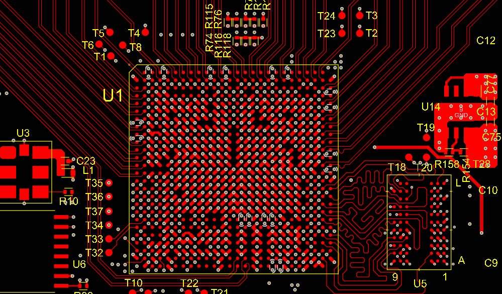
The outer two rows on this Ethernet controller BGA are used for routing to RJ45 jacks and a DDR module.
The above layout shows an Ethernet controller (U1) being routed to multiple RJ45 jacks and a DDR memory module (U5). The top layer is shown above and is used to route differential pairs from the outer rows to the RJ45 jacks, as well as single-ended length-matched traces in a parallel bus to the DDR module (see the serpentine traces in the right side of the image). All of these traces are impedance controlled with a set width in Altium’s design rules. The remaining pads in the internal rows of the BGA are for power and ground; you can spot these as thick traces are used and to connect to vias, which then connect to polygons on the inner layers. Although this BGA has ~700 connections, only a small number are being used for routing signals, and the board shown above only required 6 layers to support all signals, power, and ground (2 signal, 3 power, 1 ground).
If you’re using a rectangular BGA, use the short edge to count up your number of rows in the above formula. This is not typical outside of DDR and non-DDR SDRAM modules (see U5 above). In SDRAM modules, it’s typical to put a space between the rows of balls in the BGA to allow additional routing along the surface layer. One reason for this is that SODIMM RAM cards generally have limited layer counts (typically 4), so that leaves only 2 layers to route microstrips into dense SDRAM chips.
Once you’ve determine the layer count requirements, you can select a fanout style and size your vias.
Choose a Fanout Style
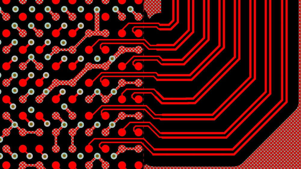
The standard BGA fanout style in a reasonably dense BGA (e.g., less than 1 mm pitch between balls) is a dog bone fanout, where small traces on the internal balls connect to vias between ball rows. This is the style used in the above image. When a denser BGA is used, the via and pad size may become so small that the fanout style will force the via to be placed directly in the solder pad for the BGA. In this case, the vias must be filled and plated over (called VIPPO) to create a solid copper pad for soldering during assembly. To determine whether via-in-pad or dog bone fanout can be used, you’ll need to determine the via size needed to route signals from the BGA footprint into the inner layer.

Dog bone fanout example for a BGA. Notice how each internal row is routed through a deeper internal layer. [Source: MacroFab]
Sizing Vias in BGA Routing
One important parameter that is sometimes overlooked in BGA routing and fanout is the size of the vias required to reach inner layers. There is an important aspect of reliability to consider here as defined in the IPC-6012 standards. As the pitch between balls gets smaller, the space available for the annular ring on internal vias also gets smaller. This eventually forces the via diameter to get smaller to continue complying with IPC-6012. Eventually, the via aspect ratio gets too large for the given via diameter, creating a DFM issue and forcing the designer to opt for blind/buried/staggered vias for routing internal rows.
At this point, the only way to relieve the DFM issue and ensure a sufficiently large annular ring is to just use via in pad. The cutoff for using via-in-pad vs. dog bone fanout is not so clear and depends on the ratio of the BGA solder pad size to the pitch, as well as the layer count and layer thickness. This is a complex problem that takes some experience as well as advice from an experienced fabricator.
Very High Density with VIPPO
In very dense BGAs with very high signal net counts, eventually the layer thickness will get so small that you might be able to route groups of differential pairs between balls. These boards may have 12 or more signal layers in order to support such a high number of signals required in the BGA breakout, but the trace width could be small enough so that you can still limit the number of layers to a manageable number. If you follow the above process and create a proposed stackup, you’ll be able to determine the required trace width and spacing needed to meet impedance and crosstalk requirements. Make sure to send your stackup in for approval with your fabricator before you start BGA routing, otherwise you’re risking a redesign once the PCB layout is finished.
One option is to take advantage of the input impedance of long transmission lines and use short sections to double BGA routing away from the external rows of the BGA footprint. This is shown below; the differential pairs in this image are routed so that the initial trace sections are very thin, allowing two traces to be routed between balls instead of one trace. This is only appropriate as long as the electrical length of the thin sections is sufficiently short, i.e., as long as the input impedance of the overall transmission line is not dominated by the impedance of the thin trace sections.
Dog bone fanout and BGA escape routing with thin trace sections.
Once you’ve broken traces out from the BGA with an escape routing style, you’re ready to route traces to the remaining components in your board. Your routing tools can do the remaining difficult work getting large groups of traces over to the required areas. Today’s ECAD software can help simplify these routing tasks and keep you productive as long as you work with an experienced design team. Smart selection of BGA components, fanout style, via sizing, and appropriate trace routing can help you implement a very aggressive form factor when needed. If you’re outsourcing BGA routing tasks to an external firm, make sure they understand how to implement high-ball-count BGAs in a PCB layout and design the stackup to accommodate these dense components.
Experienced designers can help you implement best practices for BGA routing and an aggressive form factor for a variety of systems while staying compliant with industry standards. If your company is pushing the limits of telecom, data center, aerospace systems, and low power embedded systems, it pays to work with an experienced electronics design firm. NWES helps private companies, aerospace OEMs, and defense primes design modern PCBs and create cutting-edge embedded technology. We've also partnered directly with EDA companies and advanced ITAR-compliant PCB manufacturers, and we'll make sure your next high speed digital system is fully manufacturable at scale. Contact NWES for a consultation.
Ready to start your next design project?
Our Clients and Partners


