
When you're a new designer or not a hardware design professional, there is a perception that two-layer PCBs are preferable for most products. This is due to some long-standing myths about two-layer PCBs and misunderstandings regarding the use of four-layer PCBs. Multi-layer PCBs are sometimes seen as more advanced, when in reality, they collectively make up the majority share of the PCB market.
If you are considering the development of a new electronic device and need a circuit board design, these guidelines can help you understand why a design firm may recommend a four-layer PCB. It is not with the intent to increase costs or margins but rather because the additional freedom and electrical performance allowed by a multi-layer board are often required to bring a PCB to market.
Pros and Cons of Two-Layer PCBs vs. Four-Layer PCBs
Before looking specifically at various myths associated with common PCB stackup options, it helps to look at the applications where these stackups are typically used. Engineers will evaluate these applications and see the advantages of four-layer stackups over two-layer stackups, and vice versa.
Typical Applications:
| Two-Layer PCBs | Four-Layer PCBs |
|---|---|
|
|
The differences in these applications are night and day. Obviously, more complex or advanced applications require four-layer boards. The biggest reason is the need for plane layers in the design, something which cannot practically be done in a two-layer board without sacrificing the second component layer. This would support signal integrity for high-speed signals and reduce emissions and EMI susceptibility.
Regardless of the differences between two-layer and four-layer PCBs, there are common myths regarding both types of PCB stackups, and these myths can easily lead to poor design decisions. A poor design decision doesn't necessarily mean the board won't work; the board could still function as intended, yet the end product may not pass EMC, thus preventing it from going to market.
Two-Layer PCB and Four-Layer PCB Myths
The EMI/EMC and signal integrity challenges revolving around two-layer boards have led to some popular myths regarding these PCBs. The same applies to four-layer PCBs, particularly concerning cost and manufacturing.
Myth 1: Four-Layer PCBs Are Much More Expensive Than Two-Layer PCBs
This myth is often stated by newer designers who have never manufactured or quoted a four-layer PCB. In quick-turn prototyping runs, four-layer PCBs do carry a markup due to the extra processing steps, particularly in the US. However, the extra fabrication cost is significantly lower than the cost of a failed run due to failed EMC testing and the cost of redesigns. Overseas, in some Chinese factories, two-layer and four-layer boards are often quoted at similar prices, with only a slight difference in lead time. Extending the allowable lead time further can even result in four-layer PCBs costing less than comparable two-layer PCBs.
Myth 2: Two-Layer PCBs Can’t Be Used for High-Speed Digital
There is some truth to this myth, only in that some high-speed digital interfaces can be used in a two-layer board; the rest will require four or more layers. The reason for this is the required level of shielding effectiveness around the high-speed traces in the design. In a two-layer PCB, when trace density is low enough that all IOs can be routed on one layer, a copper pour on the backside can provide enough ground to support high-speed routing. The top layer can also be filled with a pour to provide additional grounding.
In controlled impedance interfaces, such as USB or 10/100 Ethernet, you can use coplanar ground pour and bottom-side ground pour to set the trace impedance to the required value. For example, this has been demonstrated in a USB to serial module example project.

USB routing in our USB to Serial example project.
Myth 3: Two-Layer Designs Cannot Support RF
This is related to Myth 2, addressing signal integrity at high frequencies. RF signals can indeed be routed in two-layer boards, including up to very high frequencies in the gigahertz range. These need to be routed as coplanar lines to maintain reasonable trace widths. Typically, this is done as a grounded coplanar waveguide with the via fence pitch selected based on the RF signal frequency.
In fact, even in a six-layer PCB, RF lines can function similarly to those in a two-layer board since only the top and bottom layers are used to define the functionality of the antenna feed line.

RF feedline in our nRF52 example project.
Myth 4: Four-Layer PCBs Need a Power Plane
One common stackup type for four-layer boards, particularly in amateur design guides, involves the use of a power plane on one of the internal layers. While power planes are appropriate for boards that need to supply high current, four-layer boards do not always need a power plane. If not used correctly, treating a power plane like a regular ground plane for high-speed digital signals could result in higher EMI from the board edge due to poor capacitive coupling to the ground layer.
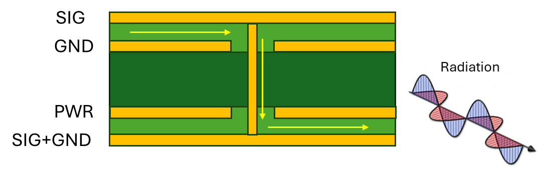
Possible radiated EMI mechanism for high speed digital signals in a four-layer PCB.
How is this potential EMI generation problem overcome? By ensuring there is enough bypass capacitance between the power and ground plane. If you rely only on bulk/decoupling capacitance to support high-speed digital signals traveling between two layers, it is possible that the power plane cannot maintain a low-impedance return path to the ground plane. To fix this, grounded copper pour can be used on the surface adjacent to the power layer, and a ground stitch via can be used alongside the signal via. Finally, high-frequency bypass caps that are normally used on digital IC power pins will aid propagation of the return path between the power plane and ground plane.
Myth 5: Four-Layer PCBs Are More Difficult to Design
Anyone who has designed a four-layer board and experienced the ease of routing traces on opposite sides of the board knows this myth is false. Four-layer PCBs with two ground planes are much easier to design because you do not need to implement orthogonal routing to prevent crosstalk. You also don’t need to worry about component density causing grounding and radiated emissions issues. In almost every case, a four-layer board is easier to layout than a two-layer board, as long as signal layers are separated with planes.
Power routing can also be very simple because large rails can be used as copper pours on a signal layer. For example, a SIG+Power/GND/GND/SIG+Power stackup is ideal for four-layer PCBs with many digital components and power regulators. This stackup allows power to be placed as copper pours that easily connect to most component pins on the surface layers with minimal effort.
Image: Four-layer PCB with power pour

Large power rails can be poured on surface layers in a four-layer PCB stackup for power routing. From our dual ADC module example project".
The Verdict
Four-layer PCBs allow for more advanced functionality, but that does not mean they are more difficult to design or build. If anything, they are easier to design than two-layer boards, especially when best practices in high-speed PCB design are followed, and plane layers are used correctly. Processing costs for four-layer PCBs can sometimes be higher, but this is often offset by slight changes in lead time. Before assuming you can only get the simplest PCBs for low prices, do your own research and shop around.
Whether you're designing high-speed PCBs for mil-aero embedded systems or a complex RF product, you should work with a design and development firm that can ensure your product will be reliable and manufacturable at scale. NWES helps aerospace OEMs, defense primes, and private companies in multiple industries design modern PCBs and create cutting-edge embedded technology, including power systems for high reliability applications and precision control systems. We've also partnered directly with EDA companies and advanced ITAR-compliant PCB manufacturers, and we'll make sure your design is fully manufacturable at scale. Contact NWES for a consultation.
Ready to start your next design project?
Our Clients and Partners


