
Applications That Need Isolated DC/DC Converters
By A Mughees • Aug 26, 2024There are many devices and applications that benefit from using an isolated DC/DC converter in the PCB.
Interactive power delivery network tool: decoupling capacitor selection, plane capacitance, BGA via inductance, and capacitor mounting analysis.
| Stage | R | L / C |
|---|---|---|
| VRM | — | — |
| Spreading | — | — |
| BGA Via | — | — |
| Plane Cap | — | — |
| Footprint | C (µF) | Qty | Layer | Orient | |
|---|---|---|---|---|---|
Log-log plot · All impedances in Ω · Ztotal (black) vs Ztarget (dashed red) · Curve names shown at line end
All values editable. Changes are session-only (not saved). Values used by the Decap Selection calculator.
| Footprint | C (µF) | ESR (Ω) | ESL (nH) | Lmnt (nH) |
|---|
| C (µF) | Bulk ESR (Ω) | Bulk ESL (nH) | Bulk Lmnt (nH) | Custom ESR (Ω) | Custom ESL (nH) | Custom Lmnt (nH) |
|---|
| Type | ESR (Ω) | ESL (nH) |
|---|---|---|
| Linear | ||
| Switcher | ||
| Custom |
| Type | Rs (Ω) | Ls (nH) |
|---|---|---|
| Ignore | ||
| Low | ||
| Medium | ||
| High | ||
| User Define |
| Footprint | C (µF) | ESR (Ω) | ESL (nH) |
|---|
| Param | Value |
|---|---|
| ESR (Ω) | |
| ESL (nH) |
| Param | Value |
|---|---|
| ESR (Ω) | |
| C (µF) |
| Material | Er |
|---|
Dielectric Layer 1
Dielectric Layer 2


Enter via and pad geometry per package size. Ltop/Lbot are computed using polynomial curve-fit coefficients. Click Calculate All to update outputs.

| Parameter | 0201 | 0402 | 0603 | 0805 | 1206 |
|---|---|---|---|---|---|
| Gap (mils) | |||||
| Width (mils) | |||||
| Pitch (mils) | |||||
| t Cu (mils) | |||||
| h diel (mils) | |||||
| A (mils) | |||||
| W_dim (mils) | |||||
| r (mils) | |||||
| B (mils) | |||||
| C1 (mils) | |||||
| C2 (mils) | |||||
| thk (mils) | |||||
| Ltop VOS (nH) | — | — | — | — | — |
| Lbot VOS (nH) | — | — | — | — | — |
| Ltop VOE (nH) | — | — | — | — | — |
| Lbot VOE (nH) | — | — | — | — | — |
Ltop and Lbot are computed using 3rd-order polynomial curve-fit equations derived from EM field solver data (Calc0201 through Calc1206 sheets in the XLS). Coefficients are embedded in the JS engine below. VOS = Via On Same side as cap pads. VOE = Via On Edge.
X2Y capacitors have 4 terminals (A, B, G1, G2). Enter geometry per package. Ltop/Lbot are computed via polynomial curve-fits from the X2Y_Mount sheet.
* Refer to figures below for detailed pad layout and dimensions


* Mounting inductance values for 'h' > 13.2 mils are extrapolated
| Parameter | 0603 | 0805 | 1206 | 1210 |
|---|---|---|---|---|
| t Cu (mils) | ||||
| h diel (mils) | ||||
| W (mils) | ||||
| r pad (mils) | ||||
| G spacing (mils) | ||||
| A-B space (mils) | ||||
| G-A space (mils) | ||||
| C1 (mils) | ||||
| C2 (mils) | ||||
| thk (mils) | ||||
| Ltop (nH) | — | — | — | — |
| Lbot (nH) | — | — | — | — |
With default inputs, X2Y 1210 package: Ltop ≈ 0.428 nH, Lbot ≈ 0.275 nH.
This PDN calculator tool is originally based on the PDN Tool V1.1.1 from Altera Corporation. Originally intended for use with Altera FPGA devices, the tool has been generalized to any processor in a PCB that pulls power from a VRM, decoupling capacitor array, and power-ground plane pair.
This tool will help users design a robust PDN for a large processor by determining an optimum number, type, and value of decoupling capacitors needed to achieve a user-defined target impedance (Ztarget) up to the target frequency of interest. The equivalent schematic considered in this analysis is shown below.
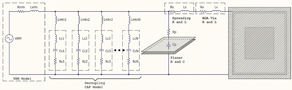
Rvrm = Resistance of Voltage Regulator Module
Lvrm = Inductance of Voltage Regulator Module
Rc1...RcN = Equivalent Series Resistance of Decoupling Cap C1 to CN
Lc1...RcN = Equivalent Series Inductance of Decoupling Cap C1 to CN
Cc1...CcN = Capacitance of Decoupling Cap C1 to CN
Lmnt1...LmntN = Mounting Inductance of Decoupling Cap C1 to CN
Rp = Sheet Resistance of Parallel Plate Capacitor
Cp = Equivalent Parallel Plate Capacitance
Rs = Effective Spreading Resistance from BGA Device to Effective Decoupling Caps
Ls = Effective Spreading Inductance from BGA Device to Effective Decoupling Caps
Rv = Effective Resistance of PWR/GND BGA Via
Rv = Effective Inductance of PWR/GND BGA Via
In the "Decap_Selection" tab:
Power integrity problems in a high-speed PCB are usually not caused by a lack of capacitance in the abstract. They come from a PDN whose impedance is too high over the frequency range where the load demands current. That is the point of target impedance. It gives you a design limit for the rail so switching events do not create excessive ripple, ground bounce, jitter, or other behavior that shows up later as a signal integrity problem. In that sense, the calculator is not just estimating capacitor behavior.
This is also why the tool includes more than capacitor value and capacitor count. A real PDN is a broadband network built from the regulator, bulk capacitance, discrete decoupling capacitors, mounting inductance, spreading inductance, plane capacitance, and the connection into the package through balls and vias. Each of those terms dominates over a different part of the impedance spectrum. At lower frequencies, the regulator and larger capacitors tend to matter most. As frequency increases, the loop inductance in the capacitor mounting structure, the BGA escape, and the plane pair begin to control the result. In faster systems, the board and package are not separate problems. They are two sections of the same power delivery path.
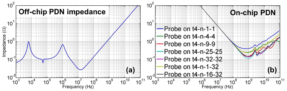
(a) PCB and (b) chip PDN contributions to impedance. [Source]
The most useful output is the impedance curve relative to the target line. If the curve stays below target, the rail has a better chance of meeting its ripple requirement during transient loading. If it rises above target, the problem is not automatically solved by placing more capacitors. A peak in the curve usually means the network has formed a resonance, and that same behavior will appear in the time domain as a stronger transient oscillation on the rail. In other words, the plot is showing where the PDN is likely to ring, not just where it has too little nominal capacitance.
| Impedance Features | Electrical Behavior |
|---|---|
| Curve exceeds target at low frequency | Bulk capacitance or regulator-side support is insufficient. |
| Sharp midband peak | Capacitor resonance and interconnect inductance are dominating the rail response. |
| High impedance at the upper end of the spectrum | Plane capacitance, BGA via path, and package-side parasitics are limiting the PDN. |
For high-speed layouts, a good PDN result usually points back to physical design decisions rather than BOM changes alone. Plane spacing, overlapping plane area, via count into the power-ground pair, capacitor package size, and mounting geometry all change the impedance curve in ways that matter more than simply increasing capacitor quantity. That is why PDN design has to be treated as part of stackup design and package escape planning, not as a cleanup step after placement and routing are already fixed.
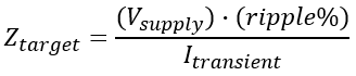
The reason we need to limit the PDN impedance below some target is because the magnitude of voltage ripple is related to the magnitude of current impulses drawn by I/Os on fast digital processors. The simple relation between these quantities is Ohm's law, where the PDN impedance is the conversion factor between current impulses and the transient voltage. This is why PDN impedance can be determined with a simple formula, which uses a voltage ripple value as a percentage of the stable core voltage and the peak current drawn by all I/Os running on the chip:
This gives a good estimate of the maximum impedance value that we can accept in the PDN. Any value below this maximum would be expected to produce a transient that, while complex in terms of time-domain complexity, maintains its amplitude within the noise margin for the I/O supply rail. As most processors have multiple rails operating at different voltages and current requirements, the same formula would apply to each rail independently (assuming separate regulators).
Once we have a target impedance design, it is possible to predict the transient response using an inverse Fourier transform, as shown in the formula below. This transform takes the input current pulse in the frequency domain and the PDN impedance spectrum, and the transient voltage can be predicted. Note that we can add a scale factor Veq to set the equivalent voltage to the stable (quiet) level required by the rail.

This is equivalent to take the convolution of these quantities using the impulse response function for the PDN impedance function (Z). Any mathematical scripting language (MATLAB, Wolfram Mathematica, etc.) can perform these calculations in the frequency domain, although the impulse response function approach has largely been taken as the standard approach in EDA software.
There are many devices and applications that benefit from using an isolated DC/DC converter in the PCB.

Heidi Barnes and Zachariah Peterson discuss the inappropriate usage of ferrite beads in a PDN in high-speed PCB design.

Learn about the design challenges and processes in PCB design for an FPGA SoM and its carrier board.


