
Material selection for high-speed PCB design is one of the most common instances where a PCB becomes over-engineered. If you look at many high-speed PCB design guidelines available on the internet, they often provide generalized recommendations and suggest advanced materials that may not always be necessary for digital systems. In fact, many high-speed PCB products are manufactured using less advanced, moderate-loss FR4 material.
When examining commercial products, you might encounter more advanced materials such as Megtron or PTFE-based materials. These material sets are necessary when channel bandwidth requirements extend into the GHz frequency range. The required operating frequency range and the available material thicknesses are two of the most significant factors influencing material selection for high-speed PCBs. Here's what you need to know about these materials, and this guide should help you match materials to different digital interfaces.
Matching High-Speed PCB Materials by Frequency
High-speed PCBs are characterized by the edge rates of signals propagating in the design and the bandwidth of physical channels used to transmit those signals. Digital interfaces in high-speed PCBs require channels to have a minimum bandwidth to transfer enough power in a signal between the driver and receiver sides of a digital interface. Because all PCB materials exhibit some absorption (insertion loss) and conductor losses, these materials ultimately limit the available channel bandwidth.
When selecting materials for high-speed PCBs, the role of the PCB designer is twofold:
- Select materials that can support the channel bandwidth an interface needs to operate
- Arrange PCB materials in the stack-up so that planes and signals are clearly defined in each layer
The second point is often easier, as the rules for constructing stack-ups for high-speed PCBs are straightforward. Alternating plane and signal layers, with many designs requiring a dedicated power layer, ensures both signal integrity and power integrity.
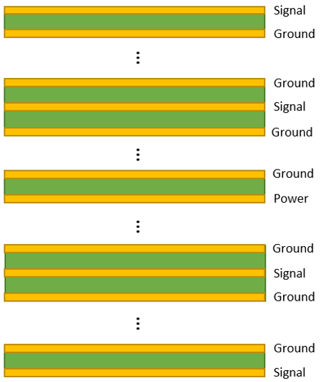
High-speed PCB stackups should be designed with alternating signal layer formats.
Choosing Dielectrics for Signal Layers
But which dielectrics should be used to support the signal layers? Most design guidelines simply recommend a low-Dk PTFE-based material (commonly Rogers) or another low-Dk material without specifying a particular product.
What actually matters is using a low-loss tangent material. It just so happens that commercially available PCB laminate materials with low Dk values tend to also have low loss tangent values. This combination helps minimize insertion loss during signal propagation. When the loss tangent (Df) is sufficiently low, the dominant insertion loss mechanism shifts to copper loss.
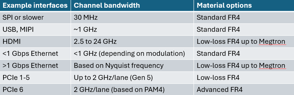
The table below illustrates typical channel bandwidth ranges supported by various material sets for some common interfaces. The channel bandwidth requirement numbers are given as values before PCB materials become limited by copper and dielectric losses.
There Is No Universal "Best" Material for High-Speed PCBs
Clearly, there is no single best material for every high-speed PCB design. Different interfaces and protocols have different bandwidth requirements. Higher channel bandwidths typically demand:
- Lower loss tangent
- Smoother copper
- Minimal variation in Dk across the channel bandwidth
Knowing the required channel bandwidth is the first step in selecting PCB materials for a high-speed design. Many designers rely on guidance from application notes, reference designs, or prior successful designs. Development boards can also be highly useful as they provide a baseline, working design with proven signal integrity.
How Much Loss Is Too Much?
A good rule of thumb for estimating the amount of loss one can accept in a physical channel is to consider one of the following, at whichever frequency it appears first:
- Lowest frequency of -10 dB return loss
- Lowest frequency of -3 dB insertion loss for the target length of your route
This is not the best metric for every design, but it provides a rough estimate of the channel bandwidth a transmission line can support.
Differential Stripline Design Example
Consider the differential stripline design example shown below. In this example, the total insertion loss per unit length has been calculated using Polar Instruments' Si9000 software. The image below shows the geometric parameters and the causally extrapolated dielectric constant variation in frequency. Clearly, there is some variation in Dk which we expect to show up in return loss and insertion loss.

Materials data (Dk = 4.2, Df = 0.02) and geometry/roughness information for Polar Instruments Si9000 differential transmission line calculation.
The insertion loss for the rough is shown below as a dB/in. value. The multiplied by the length of the transmission line. Here, we have not accounted for any vias or landing pads from any components connecting to the stripline.
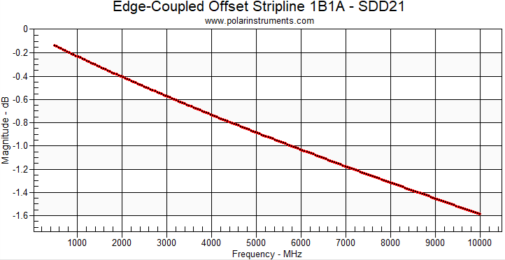
Insertion loss data for our differential transmission line.
For this example stack-up and differential stripline, suppose we want to ensure we can route up to 6 inches. The insertion loss is -3 dB at approximately 2.6 GHz. This means we could use up to 6-inch-long routes for any interface requiring up to 2.6 GHz channel bandwidth. If our interface required more than 2.6 GHz bandwidth, we could do any of the following:
- Shorten the route as this will allow more power at higher frequencies to reach the receiver
- Modify the trace design to have lower loss, such as routing with microstrips
- Use a dielectric material with a lower loss tangent
- Use smoother copper foil if compatible with the material set and PCB stack-up fabrication process
By simply swapping to an ultra-low loss laminate (Df = 0.002), the insertion-loss limited bandwidth for a 6-inch route is approximately 5.7 GHz. I’ll leave it for readers to consider how to continue extending the bandwidth further.
What About Return Loss?
This is an important point because the above estimate for insertion loss limiting the bandwidth is based on the assumption that impedance matching is perfect throughout the entire channel bandwidth. Obviously, if there is significant variation in the dielectric constants, then this cannot be the case. Therefore, variations in impedance matching also determine the level of loss in the interconnect and can limit the bandwidth.
If we look at the above differential stripline example again and plot the return loss, we can see that the impedance matching is very good at low frequencies. However, at higher frequencies, the return loss eventually hits the -10 dB limit.
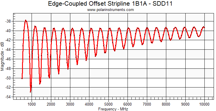
Return loss data for our differential transmission line.
Here, it should be quite clear that return loss can also be a bandwidth limiter; the channel bandwidth is effectively limited by the lower of the -10 dB return loss frequency or the -3 dB insertion loss frequency.
Evaluate Channels in Post-Layout Simulations
To verify that your material selection is appropriate for your interface, post-layout simulation work will be needed. Once the layout is finished, the channels in question should be simulated to verify that nothing in the channel creates additional limitations on the channel bandwidth. The most common bandwidth limiters in high-speed PCB design with multi-Gbps channels are vias and pads on components. We prefer to use Simbeor for these simulations as it helps balance speed, accuracy, and cost to the customer.
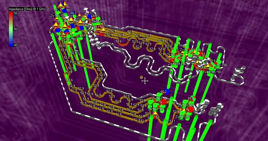
Post-layout impedance simulation of a DDR bus in Simbeor.
True channel compliance for a particular interface cannot be determined just by looking at return loss and insertion loss. Other metrics might be needed, particularly for differential channels. This could include TDR (time-domain reflectometry) measurements, mode conversion plots, eye diagrams, and crosstalk simulations or measurements where applicable. Evaluating the best material for a high-speed design is not just about focusing on the material; it's about assessing the completed routing once the PCB layout is finished.
Whether you're designing high-speed PCBs for mil-aero embedded systems or a complex RF product, you should work with a design and development firm that can ensure your product will be reliable and manufacturable at scale. NWES helps aerospace OEMs, defense primes, and private companies in multiple industries design modern PCBs and create cutting-edge embedded technology, including power systems for high reliability applications and precision control systems. We've also partnered directly with EDA companies and advanced ITAR-compliant PCB manufacturers, and we'll make sure your design is fully manufacturable at scale. Contact NWES for a consultation.
Ready to start your next design project?
Our Clients and Partners


