How Low are Dielectric Losses in Microstrip Lines?
By ZM Peterson • Aug 13, 2020Before you start routing your PCB or IC, you need to determine which trace arrangement you want to use. The three common options for digital systems are microstrip lines on the surface layer, striplines on internal layers, or arrangements of broadside coupled striplines for common-mode or differential-mode routing. Once you start working with RF systems, other types of lines are more useful.
If you look through many high speed design guidelines, especially high speed PCB design guidelines, you see a bit of a conflict about which trace geometry is desirable for use with high speed signals. The two typical guidelines are:
- Use microstrip lines as they have lower dielectric losses.
- Use striplines as the nearby plane layers provide shielding.
There is no "best" trace geometry to use in your high speed PCB, and both geometries defined above provide particular advantages. Making a proper comparison between these types of traces requires understanding why dielectric losses on microstrip lines can be lower than losses on striplines. Let’s look at this deeper so that we can see how dielectric losses are influenced by trace geometry and location in the PCB stackup.
What Determines Dielectric Losses on Microstrip Lines?
The single factor that determines dielectric losses on microstrip lines is the location where the electromagnetic field is concentrated. Whenever the electromagnetic field surrounding a trace passes through a lossy dielectric, the field will experience losses. Dielectric losses in microstrip lines are lower simply because the trace sits on the surface of the substrate. Fields surrounding the bottom half of the trace pass into the dielectric and the fringing field from the top half of the trace is the only portion of the field that interacts with the lossy dielectric substrate.
If you compare the electromagnetic field lines produced by currents on microstrips and striplines, it becomes obvious why dielectric losses in microstrip lines are lower. The image below shows a comparison of the electric field emitted from a stripline (left) and microstrip (right). Note that the magnetic field has been ignored here as PCB substrates are non-magnetic and we’re only worried about oscillating polarization and relaxation. From this image, we see that the field from the microstrip passes through air, which has zero dielectric losses until we start dealing with radar frequencies (~24 GHz and ~77 GHz, where we start worrying about scattering).

Dielectric losses in microstrip lines are lower because some field lines pass through a lossless medium (air) before passing into the dielectric substrate and terminating at the reference plane (assumed GND here). In striplines, the field lines are confined entirely in the dielectric, so they experience maximum loss. Source: T. Maleszka and G. Jaworski.
Mathematically, the dielectric constant and losses on a microstrip line are defined using an effective dielectric constant. This is defined for microstrips in the equation below. From this equation, we can see that the dielectric constant (both the real and imaginary parts) are smaller, thus overall dielectric losses in microstrip lines are smaller. Because the real part (Dk value) is lower, the signal velocity on microstrip lines is also larger.

Effective dielectric constant for a microstrip line. W is the trace width and h is the height above the substrate.
Note that there is no analogous equation for striplines. This is because the electromagnetic field surrounding a stripline passes entirely through the dielectric before terminating at the adjacent plane layer (see the diagram above). Therefore, there is no effective dielectric constant, and a signal on a stripline experiences the full brunt of dielectric losses.
Dielectric vs. Conductor Losses
When designing traces and waveguides on planar PCB substrates and semiconductor wafers, it’s important to understand the variety of effects that can produce losses. These losses are generally divided up into two areas
Dielectric Losses
The term "dielectric losses" normally refers to a very specific interaction between the electromagnetic field and a dielectric material. However, the term could also be extended to include a variety of effects that result from the interaction between the electromagnetic field and a dielectric. These include the following effects:
- DC conductance. PCB substrates and semiconductors are not perfect insulators. Current will flow between two points that are held at different potential, and this current will be dissipated as heat.
- Oscillation of bound charges (AC losses). This refers to excitation and oscillation of bound charges in the PCB substrate (or semiconductor substrate for IC designers) at reasonably low frequencies (i.e., photon energies less than the electronic bandgap). These excited bound charges experience damped oscillation and lose some energy to their host atom, which manifests itself as heat.
- Absorption. Once the frequency of an electromagnetic wave becomes large enough that the photon energy matches the electronic bandgap of the dielectric, a photon is absorbed and its energy is given to an electron. This is the basis of many optical effects and becomes important in semiconductors operating at NIR and shorter wavelengths. Note that sub-bandgap absorption is possible in nonlinear materials or through multi-photon absorption.
- Resonant power loss from fiber weaves. The glass weave in a PCB substrate can produce losses due to destructive interference under periodic loading. In effect, interference in the fiber weave cavities prevents the electromagnetic field from propagating to the receiver on a transmission line.
- Scattering. When an electromagnetic wave encounters a rough or inhomogeneous dielectric, the wave can scatter from material interfaces with differences in their dielectric constants. Regarding dielectric losses in microstrip lines, this type of effect won’t become so critical until we get to THz frequencies due to copper roughness and the glass weave in PCB substrates.
Conductor Losses
The other side of losses on PCB and IC transmission lines is conductor losses. There are three forms of losses on a conductor, which arise due to the finite electrical conductivity of all metals and the way they are deposited on planar substrates.
- DC losses. The finite conductivity of copper creates DC losses, which are easily quantified as IR drop. This source of conductor loss is always present on real conductors.
- AC losses. AC losses on a conductor arise through the skin effect, which produces eddy currents along the edge of the conductor. This then concentrates the electric field around the edge of the conductor, leading to losses with square-root dependence on frequency.
- Copper roughness. Any planar deposition process for copper produces a rough conductor. The roughness of the conductor then increases the skin effect losses, which is accounted for with a "copper roughness correction factor." Take a look at a past EDI CON presentation to learn more about copper roughness and its effects on impedance, losses, and impedance matching.
The one conductor loss that creates an additional contribution to dielectric losses is roughness of electrodeposited etched copper. This creates an effectively smaller geometry that is seen between two adjacent conductor layers in a PCB. The effect on dielectric losses as defined in a PCB laminate is shown below. Roughness as defined through the H(RMS) value increases the effective dielectric losses in microstrip lines and striplines, as shown in the model and equation below. As boards and ICs continue to push into the realm of optics (e.g., microwave photonic boards and ICs), scattering and absorption will become a major contributor to dielectric losses in microstrip lines and striplines.

Effects of copper roughness on dielectric losses in microstrip lines and striplines. Source: V. Dmitriev-Zdorov, B. Simonovich, and I. Kochikov.
Next, the roughness also impacts the losses due to skin effect by effectively increasing them. This is quantified using a roughness factor, which is multiplied onto the skin effect resistance as shown below. This value of roughness factor is frequency dependent and depends on the exact model used to describe the additional inductance and resistance due to the morphology of rough copper. The above reference provides some guidance with standard models for predicting copper roughness factors, or the roughness factor can be extracted from insertion loss measurements.
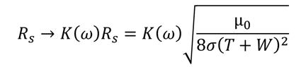
Functional transformation of skin effect resistance based on copper roughness factor.
Note that all of these effects are frequency-dependent (i.e., dispersion). Because the relevant material properties (electrical conductivity and dielectric constant) are temperature dependent, so are losses on real PCB and IC transmission lines. The fact that losses and dielectric constant in general is a function of frequency makes impedance matching for broadband signals rather difficult without using an optimization procedure that considers geometry and all sources of loss simultaneously. I’ll be presenting on this topic at some upcoming conferences with the goal of helping designers properly account for broadband losses in their transmission line designs.
NWES specializes in high speed and high frequency board design, and we understand how to account for dielectric losses in microstrip lines and striplines. We’re here to help electronics companies design modern PCB and create cutting-edge technology for a variety of industries and applications. We’ve worked with everyone from EDA software companies to defense electronics companies and the US government, and we’re always ready to take on a new challenge. Contact NWES today for a consultation.
Ready to start your next design project?
Our Clients and Partners


