PDN Impedance Analysis with Parasitic Extraction (Q & A)
By ZM Peterson • Aug 25, 2020It's time for another round of Q&A from readers. Today I’ll look at a recent question I received on LinkedIn about parasitic extraction methods for PDN impedance modeling. This is as extensive a topic as transmission line modeling, which I’ve written about extensively on this blog and for Altium. This aspect of signal integrity and power integrity (the two areas are related) has to do with properly modeling a PDN in the language of circuit models.
I have recently read the article "PDN Impedance Analysis and Modeling: From Schematic to Layout" which was written by you. I have also read many other articles from you but my main question will be from the one I mentioned. In that article, you gave an idea about modeling parasitics by calculating and gathering from the datasheet. But I wonder is there a way by which we can extract parasitics from the layout (interplanar capacitance, via and trace resistance and inductance etc.) and integrate some component model to get better results?
I will be happy to hear if you have any comments and knowledge about the subject.
Although we tend to think of PDN impedance and transmission line behavior in different ways, they are intimately related, and it is even appropriate to use similar techniques to extract parasitics for use in circuit models. Let’s look at this mathematically rich topic in greater detail.
Parasitic Extraction Methods
Before going any further, I’ll say that this is an extensive topic. The methods used for parasitic extraction for a PDN can roughly be divided into 3 areas:
- Manual calculation. Just as it’s name implies, this involves calculating parasitics directly by hand. Unfortunately, this is only tractable for the simplest PDN geometries.
- Field solvers. This involves using a full-wave field solver (ideally with an FDFD method) to calculate capacitances and inductances throughout the PDN directly. This is preferable to the previous method.
- Regression to circuit models. This is a data-driven technique, where some measurements are fit to a broadband circuit model. This is the state-of-the-art for modeling transmission lines to match experimental data, but it is not so easy to generalize to any other system. The same can be said when these techniques are applied to PDN modeling.
Of these three categories, the first is the least desired. The second is the least cost-effective, and the third method is by far the most complicated. The last two methods are both known to produce highly accurate results, and the third method provides very accurate modeling for specific systems as it is a regression-style technique. Let’s look at each of these methods in more detail to see their pros and cons.
Circuit Element Methods and Models
An upcoming article from Kella Knack on Altium’s blog recommends treating planes like a transmission line to calculate the inductance, where the sheet capacitance is used with the cross-sectional area of the power/ground plane pair and distance between them. This simplistic method would give a decent approximation of two of the parasitics needed to describe a portion of a circuit model for the PDN in a circuit board.
The problem with this is that manual parasitics calculations are only good for very simple PDN geometries. Even basic interplane capacitance calculations don’t consider the fringing field as the calculation is deduced from a pair of infinite planes (where there is zero fringing field). This method is also intractable for complex geometries; there are simply too many parasitics to consider in a real PCB layout. SPICE simulations help with the calculation time, but they still require developing an accurate model, which requires measurements or a field solver.
Circuit element methods and models involve calculating parasitic circuit elements by hand and placing them into a circuit model.
Field Solvers
The most accurate treatment uses a field solver for PDN parasitics extraction or impedance extraction (basically you are extracting Z parameters). For parasitics extraction, you can use the results to build a circuit model that helps explain resonance in the PDN impedance spectrum. This is a bit of a roundabout way to get back to a circuit model, but it accurately accounts for parasitics in your PDN. If you just calculate the Z-parameters with a field solver, you don't need to worry about extracting specific parasitics around the PCB layout. Ansys SIwave is able to do this.
Genetic Algorithms for Regression
Going the regression route requires fitting a distributed element model or lumped element model back to measurements of PDN impedance, S-parameters, Z-parameters, or anything else. These methods range in complexity and accuracy, with accuracy varying with model complexity and numerical rigor.
One accurate method used with transmission lines is to create a cascaded network model with parasitic circuit elements, which can also be used for a PDN. A genetic algorithm can then be used to extract the parasitic circuit element values for each stage of the cascaded network. This same approach is taken with transmission lines using S-parameter data, but here you're just doing it with PDN impedance measurements. Take a look at this PDF to see a procedure for modeling causal transmission lines.

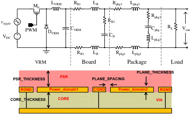
Once you fit your data to a specific model, you can recreate a PDN impedance spectrum for similar structures. PDN impedance models can be complex and often regression to a complex RLC circuit like that shown above.
Obviously, PDN impedance modeling and parasitic extraction is a deep subject that is not for the faint-hearted. If you’re in the business of creating advanced technology that requires precision power integrity, you need to work with the right design firm to help create your next product.
At NWES, we help our clients stay at the cutting edge with advanced PCB design and analysis services. We've also partnered directly with EDA companies and advanced PCB manufacturers, and we'll make sure your next layout is fully manufacturable at scale. Contact NWES for a consultation.
Ready to start your next design project?
Our Clients and Partners


