

When you’re preparing to send your PCB design out for manufacturing, the most important step is assembling a complete and accurate set of production files. Every manufacturer has slightly different capabilities, but they will still ask for the same core deliverables: PCB fabrication data, PCB assembly documentation, and a BOM. This typically includes Gerber or ODB++ files for the board layers, fabrication and assembly drawings with notes, a BOM, and a pick-and-place file for component placement.
These files translate your design intent into the data that fabricators and assemblers use to build your board. Missing or incomplete files can delay production, create confusion at the factory, or result in boards that don’t match your specifications. Understanding what each file type contains helps ensure that your design moves smoothly from layout to finished product.
PCB Fabrication Files
PCB Production Data Files: Gerbers, IPC-2581, and ODB++
When you’re ready to have your PCB manufactured, the fabricator will need a set of files that describe every physical and electrical feature of your board. These are known as production data files, and they provide the exact instructions needed for drilling, copper imaging, plating, and final inspection.
The most common production formats you’ll encounter are Gerber, IPC-2581, and ODB++. Each format defines how your circuit board should be built but they differ in how the data is organized.
- Gerber Files: The most widely used format in the industry. Each layer of the board is represented by its own Gerber file, along with a separate drill file. Gerbers are simple, reliable, and accepted by all manufacturers.
- IPC-2581 Files: A single XML-based file that combines all manufacturing data into one package. It reduces file count and helps ensure data consistency, provided your fabricator supports it.
- ODB++ Files: A structured folder or archive containing all fabrication data in an organized hierarchy. It’s similar in purpose to IPC-2581 but formatted for certain CAM tools and often used in high-automation workflows.
No matter which format you use, always include only the files your manufacturer requests, and verify that the exported data matches the final board revision. This ensures the factory receives a clean, complete dataset that can move directly into production.

CAM software is used to visualize PCB fabrication outputs from your ECAD software.
NC Drill File
An NC drill file defines every hole that will be drilled in your PCB; sometimes these are separated into different files for through-holes, blind/buried vias, and non-plated holes. These files use coordinate data to guide automated drilling machines, specifying hole locations, sizes, layer span, and whether each hole is plated or non-plated.
Most PCB layout tools generate NC drill files in Excellon format, which is widely accepted across the fabrication industry. A standard drill package usually includes:
- Primary drill file: contains X/Y coordinates and tool numbers for each hole
- Tool list: defines the drill bit diameters corresponding to each tool number
- Readme or drill map: (optional) provides a visual or tabular summary of hole sizes and types
When preparing your drill data, make sure the units, zero suppression, and coordinate origin match your Gerber settings. Including both plated and non-plated drill files (if applicable) helps the fabricator correctly separate through-holes, vias, and mounting holes during processing.
PCB Fabrication Drawings and Notes
A PCB fabrication drawing is the primary document your fabricator uses to manufacture the bare board. It communicates mechanical and material details that can’t be inferred from Gerber or ODB++ data alone. The drawing typically includes information such as:
- Board outline and finished dimensions
- Drill chart showing hole sizes, quantities, and plating status
- Layer stack-up with material types and thicknesses
- Cutouts, slots, and mechanical features
- Tolerances for dimensions, hole sizes, and hole placement
Alongside the drawing, fabrication notes define the standards, materials, and processes that must be followed during manufacturing. These notes act as the “instruction manual” for your PCB fabricator, providing both general requirements and design-specific constraints. A well-written set of fabrication notes typically includes:
- Material specifications: Core and prepreg types, dielectric constants, Tg values, and copper weights for each layer.
- Surface finishes: Requirements for finishes such as ENIG, HASL, immersion silver, or OSP, depending on the assembly process.
- Hole details: Minimum drill sizes, aspect ratios, and plating requirements for through, blind, and buried vias.
- Solder mask and silkscreen: Color, finish, and registration tolerances, as well as allowed or prohibited ink overlap.
- Dimensional and spacing rules: Minimum annular rings, edge clearances, and distance-to-copper limits.
- Quality and inspection standards: IPC class requirements, electrical testing, and acceptance criteria for cosmetic defects.
- Process requirements: Lamination cycles, baking instructions, and any controlled impedance specifications that must be verified during fabrication.
For more advanced designs, fabrication notes may also include details for microvia formation and stacking, planarity and flatness tolerances, embedded component areas, or special test coupons for quality verification. When these notes are generated directly from your PCB design tool, they ensure every manufacturing detail aligns with your current stack-up and design revision, minimizing miscommunication and rework.

PCB fabrication drawing example from our nRF52 module example project.
What About PCB Panel Drawings?
In many cases, the contract manufacturer will generate the panel layout themselves based on your board geometry, but this is not guaranteed, especially when you have special depanelization features or constraints (e.g. custom tooling, scoring or tab/routing rules). If you are asking your designer to produce a custom panel, you’ll need to provide the parameters (panel size, tooling holes, spacing, v-scores or tabs, fiducials, clearances) so the designer can build a compliant panel drawing.
PCB Assembly Files
The files required for PCB assembly only consist of three items: the BOM, pick-and-place file, and assembly drawing. These three documents are fundamental for manufacturing PCBAs, from sourcing to final inspection.
Bill of Materials
A product’s BOM is a structured list of all parts, materials, and assemblies required to manufacture a product and bring it to market.
For PCB designers, a BOM contains all the electronic part numbers that will be used in the PCB Assembly (PCBA).
Every BOM for an electronic device includes, at a basic level, the following information:
- Internal part numbers and quantities
- Reference designators for each part
- Manufacturer names, part numbers, and acceptable alternates
- Supplier names, supplier part numbers, and pricing information
For some assemblies, a BOM contains a PCB part number and materials.
The BOM is more than a shopping list; it acts as a single source of truth connecting design, procurement, and manufacturing. It’s important to have all of the part information in one place, so PCB buyers can make sense of potentially confusing information like multiple part numbers for the same component.
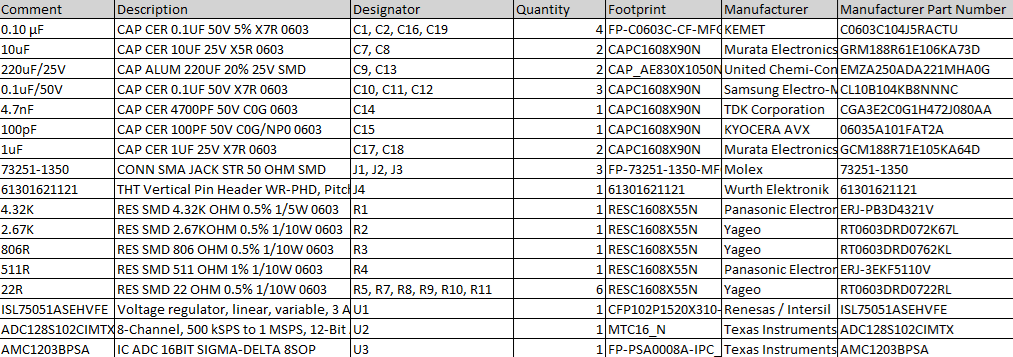
Sample bill of materials from our dual ADC module example project. These are most often exported in Excel format.
Pick-and-Place File
A Pick-and-Place file (also called a Centroid file or XY data file) tells the assembler where each component should be placed on the PCB. It lists every part’s exact X/Y coordinate, rotation, and side of the board (top or bottom). Without it, automated assembly equipment can’t correctly position parts.
A standard Pick-and-Place file usually includes the following data fields:
- Reference designator (e.g., R1, U2, C15)
- X and Y coordinates (in mils or millimeters)
- Rotation angle (orientation of the part in degrees)
- Layer side (top or bottom)
- Package type or footprint name
Most PCB layout tools can automatically export this file as a text or CSV format. Make sure to check the units and coordinate origin settings before export so they match your fabricator’s requirements. Providing an accurate Pick-and-Place file helps avoid component misalignment during SMT assembly and reduces setup time at the factory.
PCB Assembly Drawing
A PCB assembly drawing is a visual and annotated document that complements your Gerbers, BOM, and Pick-and-Place file. Its goal is to provide the assembler with additional clarity and instructions about how the parts should be integrated, in ways that can’t be fully captured in netlists or coordinate files.
While the pick-and-place gives precise coordinates, the assembly drawing gives context. It typically includes:
- A top and bottom view of the board showing component outlines and reference designators
- Reference dimensions and assembly outlines
- Orientation indicators (e.g. pin-1 markers, polarity marks)
- Hardware and mounting items (standoffs, screws, press-fits)
- Notes on soldering, inspection, cleanliness, coating, and handling
- Cautionary markings like ESD warnings or classes

Assembly drawing for our NFC reader example project.
Here’s why a PCB assembly drawing matters:
- Visual sanity check: The drawing helps operators quickly scan whether a part is missing, mislocated, or misoriented.
- Communicating special rules: For example, if a section must not be coated, or if a component leads must be bent, that can be called out in the drawing notes.
- Assembly standards & compliance: You can (and should) include workmanship standards (e.g. “assembly shall conform to IPC-A-610”), ESD handling rules, cleaning or packaging requirements, and other critical constraints.
- Ambiguity reduction: Even with excellent CAD files, misunderstandings happen. The assembly drawing acts as a “manual override” to clarify your design intent to the manufacturer.
Assembly notes define the expectations on the PCB assembler during production. Common items include references to workmanship standards (e.g., IPC-A-610/J-STD-001), soldering requirements, cleaning and inspection procedures, and ESD handling rules or standards. Notes may also specify acceptable substitutions or assembly variations, such as whether certain connectors can be hand-soldered instead of machine-placed.
For boards requiring selective soldering, conformal coating, or underfill, assembly notes clarify where these processes apply. When written clearly and reviewed against the BOM and Gerbers, these notes ensure consistent quality and reduce back-and-forth communication with the PCB assembler.
Whether you're designing high-speed PCBs for mil-aero embedded systems or a complex RF product, you should work with a design and development firm that can ensure your product will be reliable and manufacturable at scale. NWES helps aerospace OEMs, defense primes, and private companies in multiple industries design modern PCBs and create cutting-edge embedded technology, including power systems for high reliability applications and precision control systems. We've also partnered directly with EDA companies and advanced ITAR-compliant PCB manufacturers, and we'll make sure your design is fully manufacturable at scale. Contact NWES for a consultation.
Ready to start your next design project?
Our Clients and Partners



















