

The short answer to this question is yes, a PCB will need a panel drawing, or at least panel artwork, in order to be manufactured. Panel artwork and NC drill files are required to fabricate any PCB in a standard panel, and this is necessary because commercial PCB materials come in standard panel sizes.
Normally, your PCB manufacturer will generate a panel drawing. We do not always create panel drawings for every PCB project. There are exceptions to this, and we will describe some of these exceptions below. If you think you will need to create a custom panel for your PCB design, or there is something special you might want to include in a panel, the guidance on this page should help.
Outsourced PCB Design Projects Do Not Normally Include a Panel Drawing
Normally, when you engage with a PCB design services firm to outsource your PCB layout work, there is not an expectation to create a panel drawing for the PCB layout. This is not always the case, and a panel drawing could be requested as an add-on service. There are several reasons this expectation is the case:
- Tooling requirements: Manufacturers have different tooling rail requirements on panels, so a panel drawing may need to be modified before being put into production.
- Depanelization features: Depending on tooling capabilities, different manufacturers may have different constraints or allowances on the panelization, most notably for routing and the scoring.
- PCB stackup: Designs requiring impedance control or requesting specific materials might need to be changed when standard stackups or material options differ from the specification. This means the artwork needs to change, and this should be reflected in the native PCB file.
- Panels require a specific arrangement of circuit boards, but a fabrication house might be able to recommend an alternative arrangement that offers more boards per panel.
- Testing coupons: The PCB manufacturer might need to place a test coupon along one of the tooling rails in the panel.
- Specialized fixtures: We have worked with some boards where specialized test or pin access fixtures were included in the tooling rails in the panel.
Due to these points, PCB design services firms tend to omit a panel drawing from a set of deliverables unless specifically requested by a customer. Some PCB manufacturers provide panel templates which can be used to create a panel drawing. Customers can also provide a drawing template which can be populated with layer exports from the PCB layout as long as the customer panel has been pre-qualified with the desired PCB vendor.

What You Can Do With a Custom PCB Panel
Although it is usually best to leave panel drawings up to the professionals, you can still work with your PCB designer to create a panel drawing. If you want to work with your designer to create a panel drawing rather than relying on the manufacturer, you will need to gather some important inputs for the designer:
- A panel size specification or a panel template
- Any tooling requirements, such as tooling holes or minimum rail sizes
- V-score clearance recommendation for the panelization
- Milling and routing tolerances and clearances
- Any requirements or recommendations for mouse bites, such as hole size and spacing
- Number and size of fiducials to be placed on the panel
Final Thoughts
Make sure the materials that are specified in the stackup are actually available in the specified panel size. The industry has more or less standardized this, but you should still check with the fabrication house to ensure that any requested special materials for the PCB stackup are in stock or available to purchase.
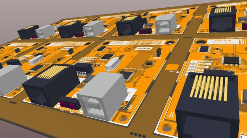
PCB panel layout in 3D shown in Altium Designer.
We have also helped customers combine multiple PCB part numbers into a single panel. This is only possible as long as the different PCBs use the same layer stack. If any of the layers are different, they cannot be combined into the same panel. This is actually one argument for relying on a standard stackup from a PCB fabricator when it will satisfy the design’s engineering requirements. Overall this significantly reduces the fabrication cost by reducing material waste.
Specialized panelization software is not required to create a PCB panel drawing. You can use a CAM software package to create the drawing from the Gerber artwork, but it is much easier to create the drawing using the mechanical layers and auto-generated drill drawing in your native CAD software. Some CAD tools support automatic generation of panels, most notably Altium Designer. If your native CAD software does not support automated panelization, you will need to use a drawing application like AutoCAD.
Whether you're designing high-speed PCBs for mil-aero embedded systems or a complex RF product, you should work with a design and development firm that can ensure your product will be reliable and manufacturable at scale. NWES helps aerospace OEMs, defense primes, and private companies in multiple industries design modern PCBs and create cutting-edge embedded technology, including power systems for high reliability applications and precision control systems. We've also partnered directly with EDA companies and advanced ITAR-compliant PCB manufacturers, and we'll make sure your design is fully manufacturable at scale. Contact NWES for a consultation.
Ready to start your next design project?
Our Clients and Partners



















