
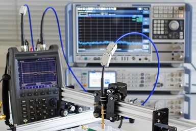
One of the simplest aspects of PCB design is most often responsible for preventing common EMC test failures: the PCB stackup. In the stackup, the layer arrangement can force layout and routing choices that contribute to EMI. However, a full understanding of the role of the PCB stackup and its impact on a grounding & routing strategy is also a contributor to a low-noise, low-EMI design.
EMC Success Starts With Your Stackup
When examining what makes a PCB stackup effective from an EMC perspective, the core function becomes clear: multilayer PCBs exist primarily to provide ground regions for circuits and signals. This may sound overly simplistic, but the majority of common EMC failure root causes directly relate to the placement and definition of ground in your PCB stackup.
We see common mistakes from early career designers that lead to EMC failure and which fail to provide signal integrity in even basic high-speed digital designs:
- New designers almost always start with two-layer PCBs, typically using single-sided placement without routing on both sides
- These simple stackups are acceptable for low density of components, DC or low-speed digital routing, and hand assembly
- Eventually, high density of components and routing leads to a lack of ground in both layers, increasing radiated emissions and EMI susceptibility
When Two Layers Aren't Enough
Successful EMC compliance in 2-layer PCBs depends on three critical factors that often work against each other as designs become more complex:
- Grounding requirements become increasingly difficult to meet as component density increases. Coplanar ground should surround traces and components on both sides of the PCB, but this becomes impossible in dense designs where components consume the space needed for ground planes.
- Component density directly impacts your ability to provide adequate ground coverage. As components take up more real estate, less space remains available for the ground regions essential for controlling radiated EMI and susceptibility.
- Signal edge rates in modern digital systems demand more sophisticated grounding approaches. When signals have fast rise times (<1 ns), more coplanar ground is needed, and ground needs to be positioned closer to signals, requiring internal planes that simply aren't available in 2-layer designs.
The breaking point becomes evident when component density reaches levels where grounded copper pour can no longer be placed around traces and components. At this critical juncture, the design enters dangerous territory for EMC failure, and the most effective solution is transitioning to a 4-layer stackup with internal ground planes.
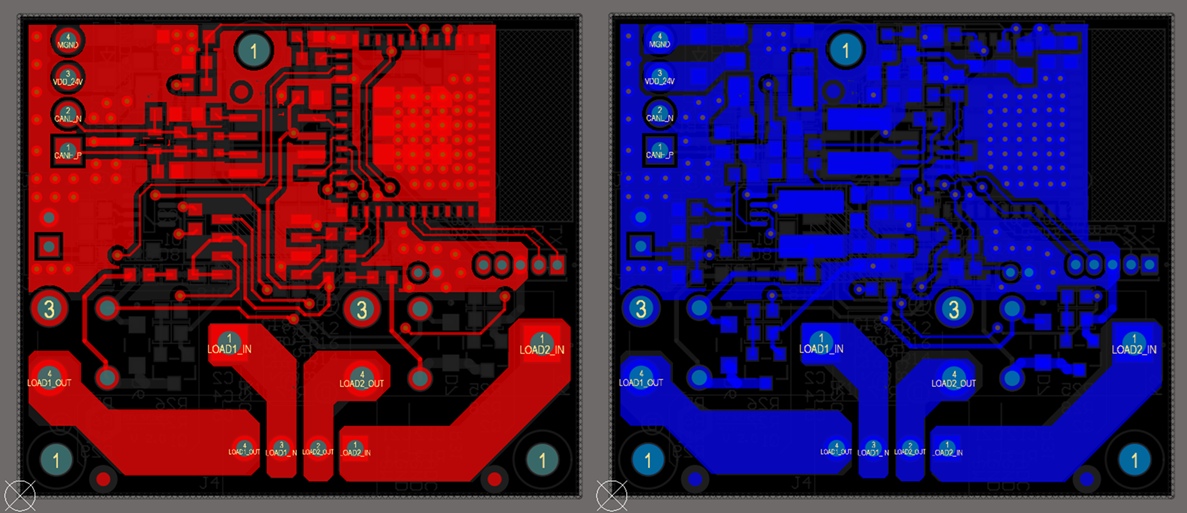
Top and bottom layers of a 2-layer PCB showing insufficient ground coverage for most of the components and signals.
Advanced Stackup Design: 4 Layers and Beyond
Basic pre-compliance testing reveals dramatic improvements when transitioning from 2-layer to 4-layer stackups. A properly designed 4-layer stackup can show approximately 10x reduction in noise compared to the same design implemented on a 2-layer stackup. This remarkable ability to control and suppress radiated emissions explains why advanced designs start with 4 layers as the minimum layer count.
For high-speed digital systems, the optimal 4-layer stackup follows a SIG/GND/GND/SIG arrangement with two internal ground planes. Power can then be routed as traces or small rails on the SIG layers. This configuration provides multiple EMC advantages:
- Controlled impedance design becomes achievable with two ground planes and thin outer layers
- Proximity benefits from thin outer layers bring ground close to signals helping control both crosstalk and EMI
- Return current management through internal ground planes connected at component pins and signal transitions via through-hole vias
The physics behind this approach centers on the relationship between digital signals and their corresponding displacement currents in the ground plane. This relationship, mediated by capacitance between the trace and plane, ensures return current remains confined to the region beneath the trace, minimizing loop inductance and keeping radiated emissions extremely low.
High-speed digital PCBs often require higher layer counts due to increased I/O requirements from processors and ASICs. High pin count components in BGA packages demand more than two signal layers for routing accessibility, while multiple power rails at different voltages and current levels drive minimum layer counts to 6 layers. The key to managing multiple power rails lies in strategic placement rather than dedicating individual layers to each rail:
- Routing large rails together on the same layer, rather than separating them across different layers
- Significantly reduces mutual capacitance while increasing self-capacitance to nearby ground planes
- This approach improves PDN impedance, directly reducing radiated EMI from board edges due to switching noise and transients
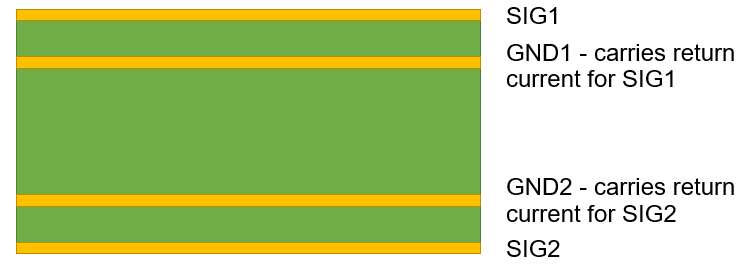
SIG/GND/GND/SIG stackup with return current locations shown.
The SIG/GND pattern can extend up to any number of layers and will give a simple way to ensure SI/PI/EMI in a more advanced design. This is the starting point for ensuring the most common emissions and susceptibility problems are addressed early in the design.
Special Considerations: Galvanic Isolation Challenges
Products requiring galvanic isolation present unique EMC challenges that demand specialized stackup approaches. Isolated DC/DC converters, common in safety-critical applications, require two physically separated ground nets occupying primary and secondary sides of transformers.
This physical separation typically creates dipole antenna effects that can radiate at problematic frequencies:
- Fast switching noise voltage between transformer sides creates oscillating electric fields
- These fields between primary and secondary ground nets result in significant radiated EMI
- Proper stackup design becomes essential for confining return currents to areas with minimal loop inductances
Common stackup approaches for galvanic isolation include:
- Simple low-current power supply modules using 2-layer PCB stackup with bottom-side ground and coplanar ground
- Integrated isolated DC/DC converters requiring internal ground planes following high-speed digital stackup principles
- Strategic placement of Class Y capacitors to provide high-frequency return current paths between primary and secondary sides
The Path Forward: Proactive EMC Design
The most effective approach to EMC compliance involves proactive consideration of stackup design rather than reactive problem-solving after test failures. Sources of EMI relate to both PCB layout and routing decisions, as well as stackup design choices. Determining whether changes in placement, routing, or stackup are necessary requires careful analysis of PCB layouts alongside understanding of signal integrity requirements and component functions.
Whether you're designing high-speed PCBs for mil-aero embedded systems or a complex RF product, you should work with a design and development firm that can ensure your product will be reliable and manufacturable at scale. NWES helps aerospace OEMs, defense primes, and private companies in multiple industries design modern PCBs and create cutting-edge embedded technology, including power systems for high reliability applications and precision control systems. We've also partnered directly with EDA companies and advanced ITAR-compliant PCB manufacturers, and we'll make sure your design is fully manufacturable at scale. Contact NWES for a consultation.
Ready to start your next design project?
Our Clients and Partners



















