
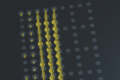
The common rule of thumb pushed by designers pretending to be high-speed PCB design experts is that vias should always be avoided on high-speed digital transmission lines. In a perfect world, we would absolutely be able to do this and we could route everything as microstrips. In reality, we simply cannot do this and we have to intentionally design vias to maintain high-speed signal integrity.
The design goals for vias in high-speed PCBs depends on two factors:
- The bandwidth requirements of your high-speed digital interface and communication channel
- Whether transmission lines are single-ended or differential
We want impedance matching to be reached within the channel bandwidth, but we also want to ensure localization up to sufficiently high frequencies.
While there are models for via design that involve closed-form equations, these are not valid at very high frequencies. There are also models for differential via impedance, some of which are based on electromagnetic field solver results. In order to design and qualify ideas for high-speed PCBs, most often an electromagnetic field solver is needed.
The trick to effectively using design approaches based on electromagnetic field solvers is knowing which of the geometric parameters to change in order to affect the via impedance spectrum and localization. This article will examine these factors in via design with an aim to target high-bandwidth channels in high-speed PCBs.
Main Goals in Via Design for High-Speed PCBs
Normally, designing vias only concerns itself with manufacturability. When vias are placed on traces for high-speed signals, we also concern ourselves with signal integrity in the via transition. The designer needs to choose a via size that is manufacturable without creating excess return losses. However, this requires some context; PCB vias only need to have matched impedance in certain frequency ranges. For example, the via on an SPI line does not need to match to a specific characteristic impedance because the channel bandwidth on an SPI line is very small.
In general, we have three requirements for signal integrity in the transitions in high-speed PCBs:
- Maintain a return current near the signal transition
- Match the via input impedance to the transmission line impedance when channel bandwidths exceed approximately 3 GHz
- At very high frequencies, place stitching vias to maintain localization of the electromagnetic field around a signal via
Which of these points becomes a priority depends on the frequency range and whether we have single-ended or differential vias.
Understanding Via Impedance and Localization
The first place to start when designing vias for high-speed PCBs is to understand what contributes to via impedance and what determines localization. Via impedance can be extracted from a return loss simulation or can be modeled directly using several approaches. Take a look at the single-ended via impedance spectrum for a differential via pair shown below, which was calculated using Simbeor.

Single-ended via input impedance example.
The single-ended via above has an input impedance spectrum that appears either capacitive or inductive in different frequency ranges. These curves can be complex in terms of shape but appear to follow a single period of the standard input impedance function for a transmission line. The green line in the above image denotes the localization frequency, which is the maximum frequency at which the via can contain the electromagnetic field around the via barrel. Above this frequency, the via can radiate and nearby circuits can experience strong crosstalk from the via.
High data rate channels requiring multi-GHz bandwidth are predominantly differential. An interface might be source synchronous with parallel lanes, such as CSI-2, but the individual lanes in the bus are still differential pairs. This requires designing differential vias which can provide the required impedance over a broad frequency range. The rules for designing differential vias are similar to the rules for single-ended vias, but the design parameter space is different due to the spacing between the differential vias.
My approach has always been to design the via based on the channel bandwidth the via needs to support. Based on the above graph for the single-ended via, we can already identify two broad frequency ranges for via impedance: below approximately 3 GHz, and all frequencies above this value.
PCB Via Impedance Below 3 GHz Channel Bandwidth
At less than 3 GHz, it is clear from the above graph that the input impedance looking through the via in standard thickness PCBs will be matched to the output trace impedance. In other words, the via impedance does not matter in this frequency range. This is equivalent to stating that slowly changing signals will not experience strong reflections from the via impedance mismatch. In this case, the designer only needs to implement two possible approaches:
- Single-ended vias: place a grounded stitching via near the signal via to provide a return path during the layer transition; enforce the standard via-to-copper clearance rule in your ECAD software
- Differential vias: maintain symmetry in the trace entry where possible and maintain the spacing between the vias to prevent any skew or mode conversion along the layer transition
Aside from these points, no additional design steps are required.
3 GHz to Approximately 30 GHz Channel Bandwidth
Single-ended and differential vias operating in this frequency range must be impedance matched to the transmission lines on each end of the via. The typical localization limits in the approximately 40 or 50 GHz range still apply in these vias, even when implemented as through-hole vias.
At these frequencies, the designer primarily forms a structure like the options shown below for a single-ended via or differential vias. The location of the stitching vias is such that the anti-pad will be the main factor determining impedance in most via designs. For stacks of blind/buried vias, the layer thicknesses and any cutouts below landing pads also impact the via impedance.
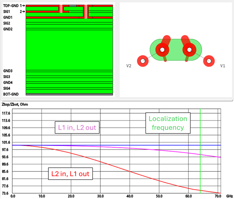
Differential via impedance spectrum example.
These vias have an S11 curve shown below (only L1 in/L2 out is shown). The impedance mismatch becomes apparent at higher frequencies (around ~30 GHz).
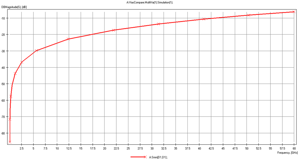
S11 for the above differential vias.
My experience has been that these frequency ranges typically require an appropriate size anti-pad; a dense array of stitching vias is not needed to ensure localization. Only a small number of appropriately placed stitching vias will set the localization frequency around approximately 40 GHz. This occurs when the stitching vias are placed farther than the edge of the anti-pad, which is almost always the case in practical PCB layouts.
Above 30 GHz Channel Bandwidth
Above 30 GHz, we can no longer simply place a few stitching vias near the signal via without considering the distance. The distance to the stitching vias may need to be adjusted in order to set the localization frequency higher than the channel bandwidth. The anti-pad size, and the via spacing in differential pairs, will also need to be adjusted to ensure the target impedance is reached up to higher channel bandwidths.
Another factor impacting the impedance of a via transition is the layer where the signal lands, such as a microstrip to stripline transition. The distance to ground above and below the signal land can impact the impedance, requiring cutouts below the land or an adjustment of the layer thicknesses to extend the valid impedance range across the channel bandwidth.
Consider the vias shown below, which were designed as part of a 112G-PAM4/224G-PAM4 transceiver design, without any cutouts above/below via landing pads. These vias are connected to a microstrip and stripline at nominal 98.5 Ohms impedance (100 Ohms with 1.5 Ohms loss compensation).
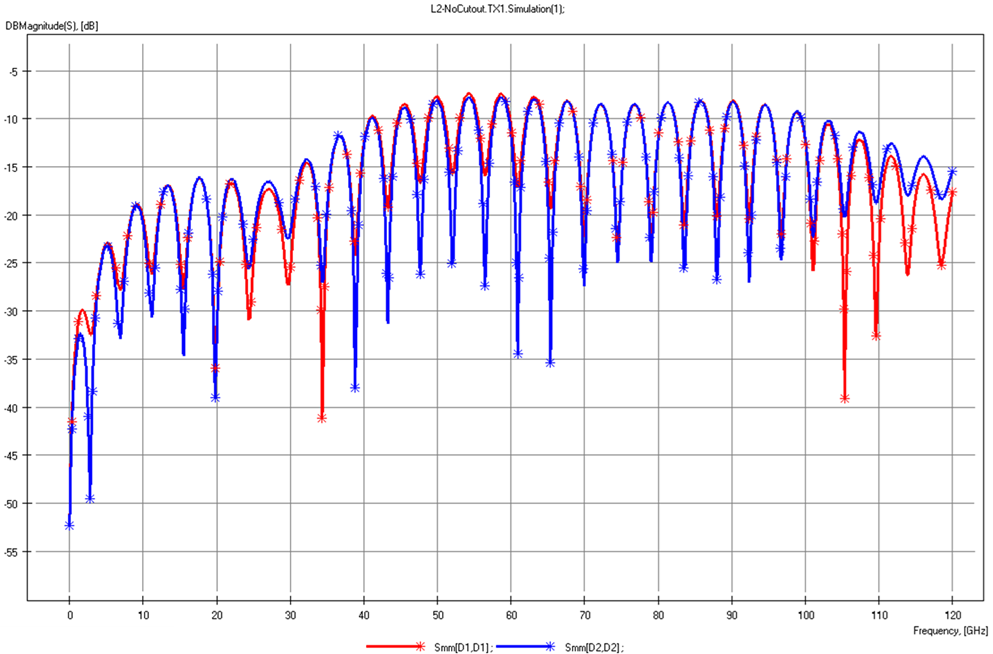
Differential vias with design targeting 112G-PAM4 channel.
What ultimately matters in these via transitions is the S-parameters for the entire link. The S-parameters for a 1-inch differential stripline with these vias at each end gives sufficient bandwidth for 112G-PAM4, but the return loss is out of spec for 224G-PAM4. By simply applying a ground cutout below the via landing pads, we can somewhat compensate for the high capacitance present at the component lands and improve the S-parameters as shown below.
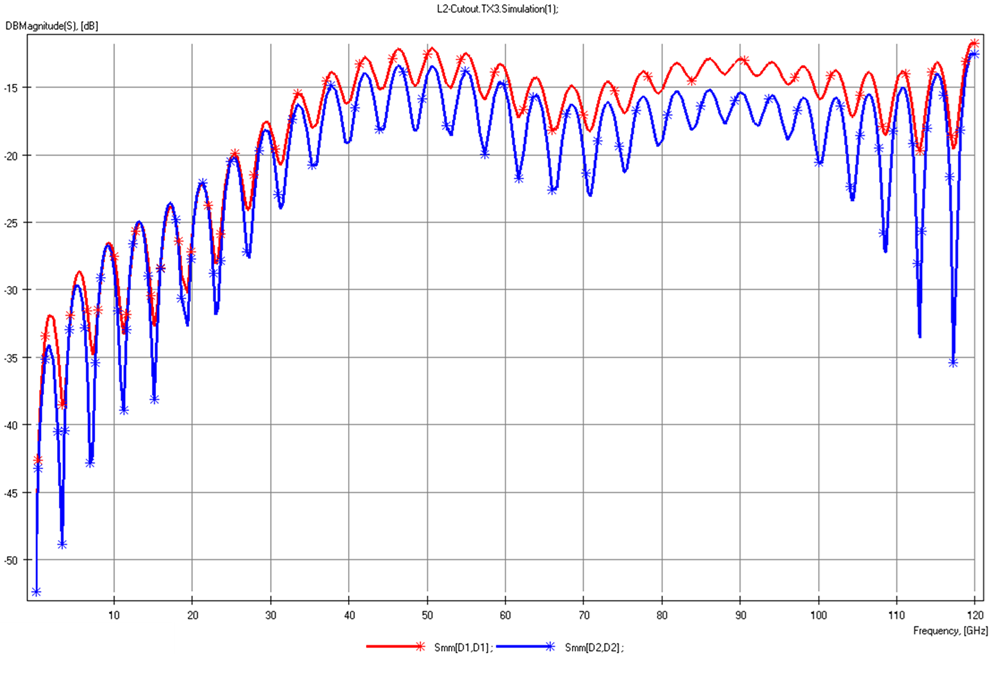
Differential vias with improved S-parameters by adding a cutout below the via landing pads. If we take -10 dB as the acceptable return loss limit, these vias would support 224G-PAM4 signaling.
At these frequencies, it should be clear that all available levers need to be pulled to fully optimize vias. In many cases, you will never get the impedance of the via perfect and there may be large remaining deviations from the target impedance in different frequency ranges. Ultimately what matters is the S-parameters of the entire set channel; as long as the vias do not cause the full channel S-parameters to exceed reflection and loss limits, then the vias will be acceptable.
The graph below shows the insertion loss that is possible for a reasonably well-matched via. The corresponding impedance spectrum of the via is also shown. It should be clear that the insertion loss in the range where the impedance match is very good (at low frequencies) is quite low, as low as 0.1 dB. At much higher frequencies, where impedance match is more difficult, the insertion loss increases to 0.5 dB in the 50 GHz range.
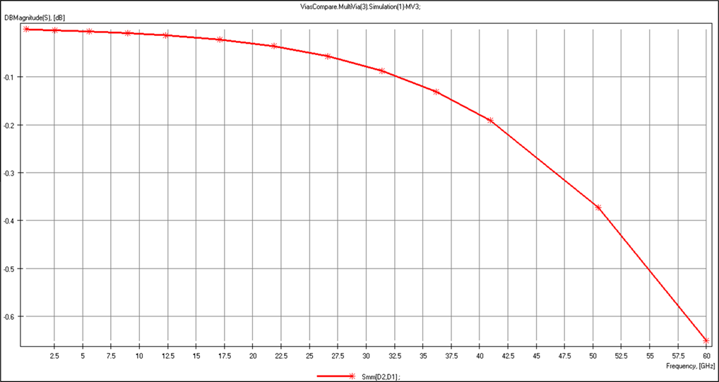
Insertion loss for the above improved differential vias example.
In the past, I have seen a variety of numbers quoted for via insertion loss. Some well-known instructors on high-speed design topics will claim that via loss will be as much as 0.5 dB or 1 dB at frequencies as low as 10 GHz. These numbers are only possible when the impedance match between the via and transmission lines is extremely bad. A well-matched via could have much lower insertion loss, but of course this is a function of frequency.
What Impacts the Localization Frequency?
I mentioned localization several times above. This is an important characteristic of via structures as it determines at what frequency the transitioning signal starts to radiate from the edge of the via structure. The localization frequency is in the 10’s of GHz range and depends heavily on the geometry of the via structure. In particular, the via localization frequency depends strongly on:
- Antipad diameter around the signal via
- The location of stitching vias
- The number of stitching vias
A simple example illustrates why high-speed design "experts" who claim that stitching vias do not matter for signal propagation through a via structure are wrong, especially where differential vias are concerned. Take a look at the single-ended via below, which can support signal propagation into the 10-20 GHz range. When 2 stitching vias are used, the localization frequency is near 25-30 GHz. When 4 stitching vias are used at the same radial distance to the signal via, the localization frequency increases to ~48 GHz.
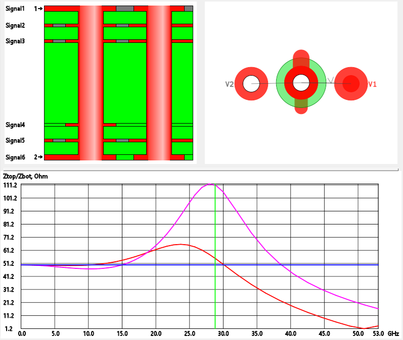
Via localization illustrated with 2 stitching vias.

Single-ended via with 4 stitching vias and higher localization frequency.
Similar results are seen with differential vias, something which I have shown repeatedly in articles on Altium’s blog, in my high-speed design seminars, and in training sessions. This is because the stitching vias start to make the via structure look like a coaxial structure, which has a TEM cutoff frequency determined by the location of the outer conductor (in this case, the stitching vias are analogous to the outer conductor). This is why BGA ball pitch determines the TEM cutoff frequency and is a reason why 224G-PAM4 channels require a maximum BGA ball pitch of 0.8 mm to ensure TEM propagation.
- To learn more, read my article on Altium Resources: How BGA Pin Pitch Impacts Signal Integrity at 224G-PAM4 and 448G
How Teardrops Affect Signal Propagation
One feature that can be added to vias to potentially aid impedance matching is teardrops. Teardrops are normally used to compensate for drill wander, particularly in Class 3 designs, where the goal is to ensure sufficient annular ring for Class 3 compliance after drilling. Teardrops also have an impedance matching effect when examined at gigahertz frequencies. As is always the case with copper features on a high-speed PCB, smaller copper features become more apparent at high frequencies, and thus one would expect a greater effect higher in the channel bandwidth.
Tapers generally flare out from a trace in order to match to a low impedance load. Therefore, if a particular via appears capacitive, the taper might improve impedance matching looking into and out of the via. Whether this is actually effective in the channel bandwidth you need requires evaluation with S-parameters. Following this evaluation, one can quickly judge whether the impedance match improves in the relevant frequency range.
High-Speed PCB Design Tools for Success
Unfortunately, there are no analytical formulas which provide exact answers in every frequency range. In fact, the frequency range where you need impedance matching on vias is inaccessible with analytical formulas published in Dr. Howard Johnson's textbook, which is often cited for its via impedance model. In fact, Dr. Johnson admits in his own textbook that the model is wrong and should not be trusted at the high frequency ranges where via impedance matching is needed.
For vias operating above 3 to 5 GHz, there are tools that use proprietary models, reduced field solvers, or full-wave 3D field solvers. The two best tools are SI 9000 from Polar Instruments, and Simbeor from Simberian. Consider adding these tools to your repertoire if you do not have the budget for a full-wave 3D field solver like CST or Ansys.
Whether you're designing high-speed PCBs for mil-aero embedded systems or a complex RF product, you should work with a design and development firm that can ensure your product will be reliable and manufacturable at scale. NWES helps aerospace OEMs, defense primes, and private companies in multiple industries design modern PCBs and create cutting-edge embedded technology, including power systems for high reliability applications and precision control systems. We've also partnered directly with EDA companies and advanced ITAR-compliant PCB manufacturers, and we'll make sure your design is fully manufacturable at scale. Contact NWES for a consultation.
Ready to start your next design project?
Our Clients and Partners



















