
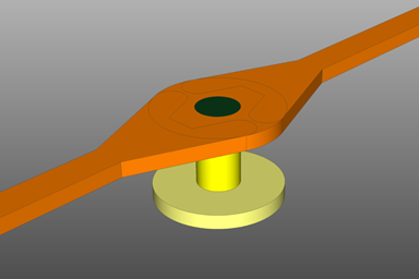
IPC standards for various types of printed circuit boards, most notably the IPC-2221 and IPC-6012 standards, define fabrication acceptance criteria for three classes of PCBs. A Class 3 design is designed and built to have higher reliability than PCBs for commercial products. These designs are intended for use in military, aerospace, healthcare, and many other areas where downtime or electrical failure could result in loss of human life. The manufacturing acceptance criteria filter down to the PCB design, where certain practices are prescribed to help ensure maximum reliability.
The most common design aspect where PCB designers focus on ensuring reliability is in via design, specifically the pads and annular rings on vias. Depending on the size of the pad and hole size for vias, some fabrication houses will recommend adding teardrops to prevent breakout or severing the signal trace from the via pad. This is where we sometimes see a debate about the use of teardrops on SMD pads and via pads for Class 3 designs. We will explore this debate in this article.
Teardrops and Via Pads in PCB Routing
In a Class 2 or Class 3 PCB, the drilling process always leaves behind some copper on a via landing pad, known in IPC standards as an annular ring. Class 2 and Class 3 designs require some minimum amount of annular ring to be left over after drilling. It is a PCB fabrication company’s responsibility to determine their positional tolerances for NC drilling during fabrication. Based on the positional tolerances for drilling, the manufacturer can then specify a minimum pad size on all plated through holes based on the drill diameter.
According to the IPC-6012 standard, the minimum annular ring left over on PCB vias must be given by the values in Table 3-5 from the IPC-6012 standard.

Table 3-5 with annular ring requirements from the IPC-6012 standard.
Note that the values in the table depend on the producibility classification for the PCB fabricator. If the fabricator has smaller positional tolerance, the required pad oversize on vias and through holes is also smaller in order to maintain the minimum annular ring.
The point of having minimum annular ring is to prevent breakout from the pad and to ensure some minimum level of copper is left over on the pad after drilling. Having the additional copper also reduces the chances of severing a trace from the pad.

Breakout on vias results when the pad size is too small or there is not enough connected copper to account for drill wander from the via pad.
One thing we have seen from fabricators is they may demand placement of teardrops on vias to ensure there is enough copper to prevent breakout and avoid severing a trace. From the above table, it should be clear that teardrops are not required to achieve Class 2 or Class 3 compliance. As long as the fabricator can produce the vias successfully, then the boards are considered acceptable.
Despite this, there are some reasons to include teardrops, including on Class 3 designs:
- When the trace is smaller than the via drill diameter, a teardrop will essentially eliminate any chance of a drill hit severing a trace
- Using a teardrop to reach Class 3 acceptability may be a simpler design change than modifying all via pad sizes
- Teardrops can also be used alongside decreasing via drill size, which may also help reach Class 3 compliance
In conclusion, while we do not view them as mandatory, they can become mandatory based on guidance from a fabrication house. There are other factors to consider when placing a teardrop, specifically related to signal integrity.
Teardrops on High-Speed and RF Transmission Lines
Anyone familiar with trace and pitch will know that modifying trace width will affect trace impedance. Teardrops essentially widen out a trace as it comes into a via, decreasing the trace’s impedance on the approach to the via. How does this impact the performance at high speeds / high frequencies?
Teardrops on a PCB are essentially short tapers. Flaring out the trace width into a via pad is essentially the same as applying a short taper to a transmission line. These short tapers can provide an impedance matching function when routing into a capacitively loaded via.

Teardrop with impedance values marked.
For example, consider the via shown below. This via drops to low impedance in the 10-15 GHz range due to capacitive loading along the via barrel from the ground plane layers. These plane layers add some capacitance to the via’s input impedance, unless the input impedance at high frequencies also appears to be capacitive. We might expect decent matching to the via’s input impedance in this range. However, at higher frequencies, the via’s input impedance looks strongly inductive and we would expect worse impedance matching due to the presence of the teardrop.
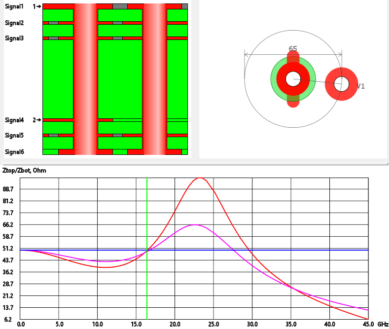
Via with low impedance due to capacitive loading.
The teardrop applies some impedance matching in these mid-range frequencies, but the frequency range depends primarily on the length of the taper. For those familiar with taper design, you will know that shorter tapers apply their impedance matching at higher frequencies.
This means you can apply a teardrop to a via on an RF signal line and avoid creating significant deviations in the impedance looking into the via transition. However, you need to have a field solver to verify that this really works in the frequency range of interest. Field solvers with via models, such as Simbeor, are capable of this calculation and can be used to determine S-parameters of the via transition.
What About Teardrops on SMD Pads?
Another area where teardrops are sometimes applied automatically by CAD tools is on SMD pads. An example in Altium Designer is shown below.
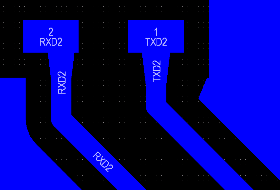
Teardrop on SMD pad in Altium Designer.
In our view, teardrops do not provide any major benefit on SMD pads. You can make an argument for improved reliability in cases of hand soldering or rework, but for standard reflow processing we have not seen a case where teardrops are needed. Our fabrication partners have also never recommended we add teardrops on SMD pads, only on via transitions, particularly for Class 3 designs.
Whether you're designing high-speed PCBs for mil-aero embedded systems or a complex RF product, you should work with a design and development firm that can ensure your product will be reliable and manufacturable at scale. NWES helps aerospace OEMs, defense primes, and private companies in multiple industries design modern PCBs and create cutting-edge embedded technology, including power systems for high reliability applications and precision control systems. We've also partnered directly with EDA companies and advanced ITAR-compliant PCB manufacturers, and we'll make sure your design is fully manufacturable at scale. Contact NWES for a consultation.
Ready to start your next design project?
Our Clients and Partners



















