
How Via Inductance Affects Signal Integrity at High Frequencies
By ZM Peterson • Dec 16, 2020When you’re designing a new PCB, you’ll need to route on more than one layer on all but the simplest of designs. Vias are the standard structures for layer changes during design, and PCB design applications have made it exceedingly easy to route into multiple layers on a PCB. But just because it’s easy to route between layers doesn’t mean that you should.
Via inductance and parasitic with respect to other conductors will affect signal integrity in different ways, depending on the frequencies involved. Since vias are inevitable in modern PCB designs, how can a PCB designer ensure their new board will operate correctly in the required frequency range? If you know how via inductance affects signal behavior, it becomes easier to judge when and how many vias to use on high speed/high frequency interconnects.
Modeling Impedance Due to Via Inductance
If you start looking through the literature, you’ll find at least 2 different theoretical (semi-empirical) descriptions of via inductance in terms of the via length and radius. Via inductance can be determined empirically, or by approximating the structure as a simple cylindrical conductor. The two prominent equations for via inductance are shown below.

Eq. (1): Via inductance equations presented by Howard Johnson (top) and by Goldfarb and Pucel (bottom).
The second equation is more accurate as it includes an extra correction factor. These equations rely on a particular approximation, namely that the inner diameter is nearly equal to the outer diameter. They also always assume that the via is electrically short, which is only appropriate up to mmWave wavelengths (e.g., ~10 mm for a through-hole via in FR4, or about 15 GHz). Finally, by considering the via inductance and resistance, we have the total impedance of the via assuming any capacitance to the reference plane is negligible:

Eq. (2): Via impedance due to via inductance, DC resistance, copper roughness (K), and skin effect resistance.
The problem with this equation is that, in reality, there is some capacitance back to some reference plane, which is the case for any conductor. Therefore, the via acts like a very short transmission line section. It will have some return loss and insertion loss, and its S-parameters can be measured. No matter how the via inductance is calculated, different sections of an interconnect will have different input impedance values along the length of the line.
Because a transmission line with vias will basically have an impedance discontinuity along the line, we have the following sources of signal loss on the interconnect:
- Return loss. There may be some mismatch between the input impedance of the (via + line) section and the input feedline section. This creates some return loss due to resulting reflection.
- Insertion loss. Copper used to form the via will have some roughness, and the roughness will loss due to depend on frequency and the dimensions of the via due to the skin effect. This creates some insertion loss.
- Resonant losses in stubs. If there is a stub on the via, this stub can also act like a transmission line branch with open circuit termination, and some signal power can branch off the main line and into the stub. If the stub is sized just right, the transferred signal can resonate, just like a typical transmission line section.
It can be difficult to see the various electrical sources of impedance and transmission line behavior on a via without looking at the via’s structure. These parasitics, particularly parasitic capacitance, are what determine the transmission line behavior observed in mmWave PCBs. The parasitics along a via can be seen more clearly when we look at the structure of a via.
Via Inductance and Capacitance
The image below shows were parasitics arise in a real PCB via. The via inductance and resistance are shown along the length of the via, which accounts for the impedance defined above in Eq. (2). Here, we have a complex capacitance across the via barrel, which accounts for the loss tangent and capacitive coupling between each side of the via barrel. If there is any nearby conductors outside the via barrel, there is also capacitive coupling to the nearby plane. In addition, the pad connected to the via will also have capacitive coupling to the nearby plane. We could draw similar images for blind/buried vias, and for filled/plated-over vias.

Structure of a typical through-hole via with parasitic elements marked in the via and surrounding reference plane/pad.
The point here is not necessarily to create a circuit model for a through-hole via. Rather, it is to show that the via’s characteristic impedance, and thus the input impedance for a (via + transmission line) section, are more complicated than just looking at the via inductance. At low frequencies, will be electrically short and thus the input impedance of a (via + transmission line) section will appear to be the characteristic impedance of the transmission line only.
An impedance simulation for a through-hole via in a 6-layer stackup is shown below. Above about 3-5 GHz, the via impedance diverges due to the via inductance, and we would expect strong reflection at midrange frequencies. Eventually, the capacitance in the via structure takes over and the impedance becomes very small. In any case, a simple through-hole via is not suitable above about 3-5 GHz.

Although the via inductance causes a divergence in the via impedance, the inductance can be compensated with some additional capacitance. This is accomplished by applying stitching vias around the main via barrel, and by adjusting the size of the antipad opening in the plane layer. As we can see in the example below, adding some vias and adjusting the antipad allows the via impednace to stabilize more closely around the target value (50 Ohms in the example below).
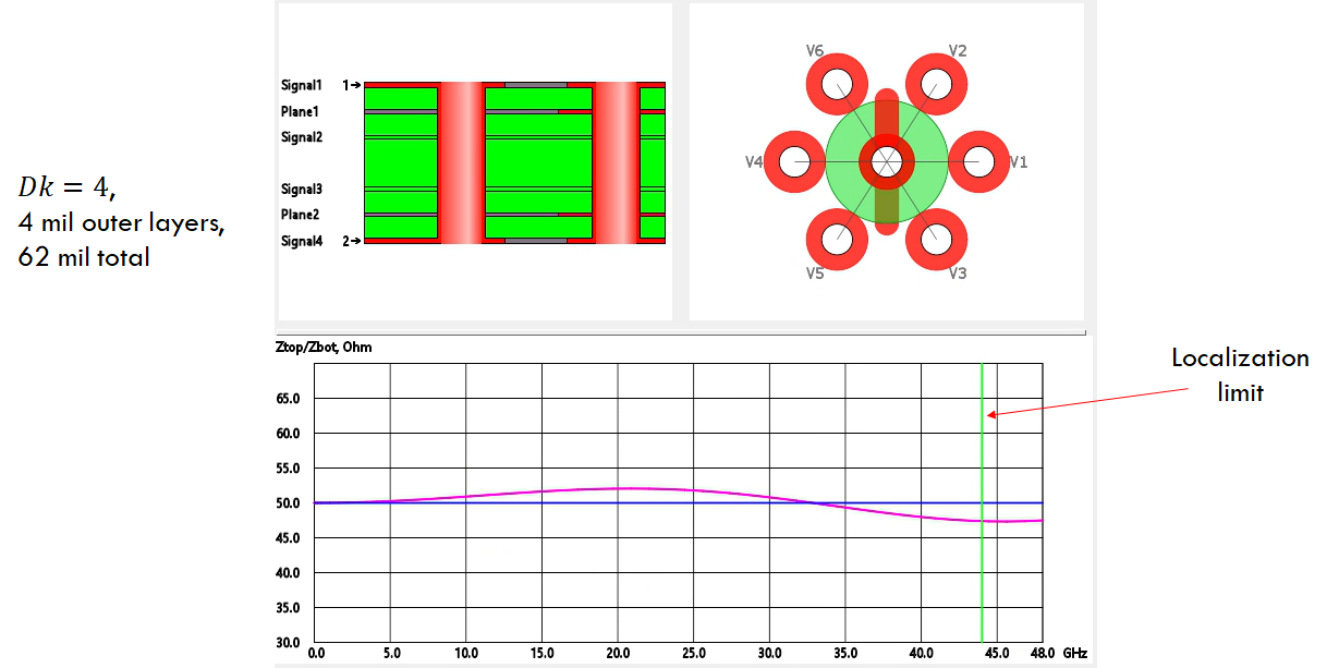
From the above graph, we see that a single through-hole via can indeed support routing up to the 40 GHz range, which is much higher than many high-speed PCB design guidelines or RF PCB design guidelines would have you believe. For differential pairs, the via transition tends to be much more sensitive to the antipad size unless the vias are separated and surrounded with stitching vias as I've shown above.
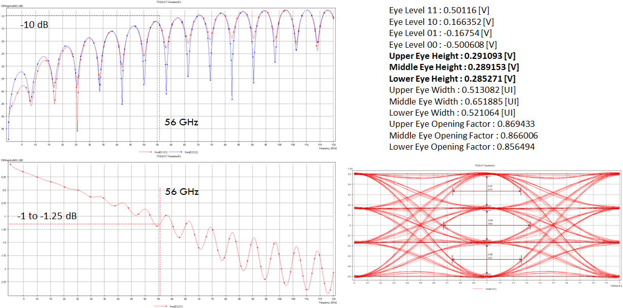
If we can further control the localization and impedance out to higher frequencies, then the via can be made suitable up to some of the most advanced technologies and fastest signaling standards. The same applies to RF systems operating above ~40 GHz, such as the 77 GHz automotive radar band. The example below shows a 224 Gbps PAM-4 channel designed by the author for use in a substrate-like PCB; the via structure was built from a stacked blind microvia/buried drilled via arrangement.
What About Backdrilling?
Another factor affecting via impedance is the total via length, as well as the presence of a via stub. These elements impact the input impedance looking into the via as a function of frequency, as well as the insertion loss, leading to dips in the insertion loss spectrum in the high GHz range (~10 GHz or higher). Stubs are very simple open quarter wave transmission line elements that result in destructive interference in the incoming signal; make sure you understand how to calculate those frequencies as it is a very elementary wave physics problem.
At sufficiently high frequencies, the via stub may no longer be electrically short, and it will modify the input impedance of a (via + transmission line) section. In the case where a via stub is present, the via could be backdrilled to minimize the remaining stub length. However, in some designs where backdrilling is applied in through-hole vias, this will not be enough to suppress reflection at the via input, and instead a blind/buried via stack will be needed. The idea in either case is to set the input impedance of the stub section to infinity to ensure that no power is transferred into the stub, thus the input impedance to the via body will ideally be matched to the line impedance. In the event where a backdrilled through-hole via does not match to the line impedance up to the required frequency limit, try using blind/buried via stacks to ensure impedance matching.
At NWES, we provide PCB design and layout services to SMBs, large enterprises, and aerospace and defense electronics companies. We know how to deal with via inductance, high frequency parasitics, and major signal integrity problems in advanced RF systems, high speed backplanes, power systems, IoT devices, and much more. We’ve also partnered directly with EDA companies and multiple ITAR PCB manufacturing firms, and we help our clients get through the PCB manufacturing process with ease. Contact NWES for a consultation.
Ready to start your next design project?
Our Clients and Partners


