
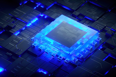
In the past, substrate-like PCBs were essentially chip-on-board designs with wirebonding taking the place of a traditional lead frame or wirebonded package. As time has gone on, substrate-like PCBs are providing high-density interconnections to semiconductor dies, essentially acting as very large substrates. However, they also play the same role as a printed circuit board as they can support soldering of off-the-shelf components in standard packaging. This dual role as an IC substrate and a PCB is unique to substrate-like PCBs, particularly when these designs are built with very fine line width and spacing of copper traces.
Although today's substrate-like PCBs push the limits of copper features and integrate semiconductor dies, they are not new products. Some of your favorite consumer products have relied on substrate-like PCBs for nearly a decade. Consumer electronics has been a big driver of maturation, but now that same drive for greater future density and compute is pushing into other industries and markets. This positions substrate-like PCBs as a new platform for high-density, highly advanced devices.
What You Can Build with Substrate-Like PCBs
Today they are being used as a replacement for 2.5D integrated circuit packaging that also allows assembly of traditional off-the-shelf components into a single device. The earliest use of substrate-like PCBs is in chip-on-board fabrication and assembly. In chip-on-board designs, the PCB also functions as a substrate for the semiconductor die, where a semiconductor die was wirebonded to a PCB and encapsulated. Interconnects would then flow to other components and integrated circuits.
Today, substrate-like PCBs have become more elaborate, where the design is used for bumped semiconductor dies, flip chip, and even 2.5D packages with an interposer. These designs eliminate wirebonding and they eliminate traditional organic IC substrates in favor of a multi-layer high-density PCB as the substrate platform. Bumped dies are then assembled onto the PCB in a standard process, and the remaining off-the-shelf components can be soldered using reflow processing.
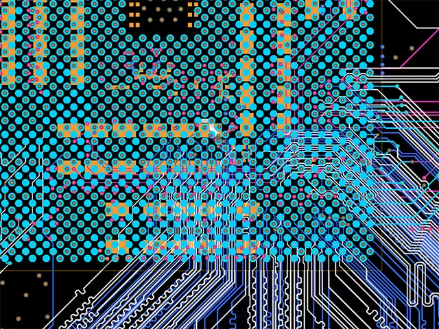
Substrate-Like PCBs and Data Center Infrastructure
Regarding today's technological shift to higher compute applications, we can't bring up substrate-like PCBs without bringing up data center infrastructure and AI. The current data center infrastructure being implemented in 2025 and 2026 runs on 224G-PAM4 data rates per lane, which aggregates to 1.6 TB Ethernet for interconnecting servers for AI compute. Next generation will double the data rate and will operate at 448 Gbps per lane, aggregating across eight lanes to 3.2 TB Ethernet. These data rates require such high channel bandwidth that it becomes unlikely traditional package and PCB stacks will be able to allow signal transmission.
This leaves two approaches for interconnects running at 448 Gbps per lane:
- Using co-packaged connector modules
- Using near-chip connectors sharing the same substrate as the semiconductor die
Both of these solutions are equivalent to using a connector module on a substrate-like PCB. Such large packages have already become the norm for the most advanced GPUs, so we should not be surprised when the same packaging design approach is implemented for networking.
UHDI Capabilities Required for Advanced Substrate-Like PCBs
Substrate-like PCBs effectively use smaller features at higher density, requiring a shift away from standard subtractive etching. The process and the required capability are both different from standard low-density PCBs and high-density PCBs.
What capability is required for some of the most advanced high-density dies in substrates or substrate-like PCBs? Typically, we require the following fabrication capability on an organic interposer or substrate:
- Linewidth and spacing down to 10 microns
- High precision etching capabilities below 1/2 oz copper
- Via formation at 1 mil diameter or less
- Low press-out thickness variation in build-up layers
- Extremely low misregistration in build-up layers
Materials are another critical aspect of these products, and they are often the same materials intended for use in IC substrates. Substrate-like PCBs require thin build-up film layers which are compatible with additive processing and laser drilling. These thin layers are required to build up the very small interconnects which are needed for routing on multiple layers. These materials are laser processable and very thin, such as below 3 mil thickness, enabling low aspect ratio laser drill microvias.
The available material sets from well-known vendors have been expanding recently thanks to the more globalized push for UHDI fabrication capacity. In the past, the UHDI build-up layer would be a build-up film material such as ABF. Today, materials like liquid crystal polymer (LCP) are being used more often for flexible substrates, and new advanced resin-coated copper materials are being introduced with low Dk and low CTE values.
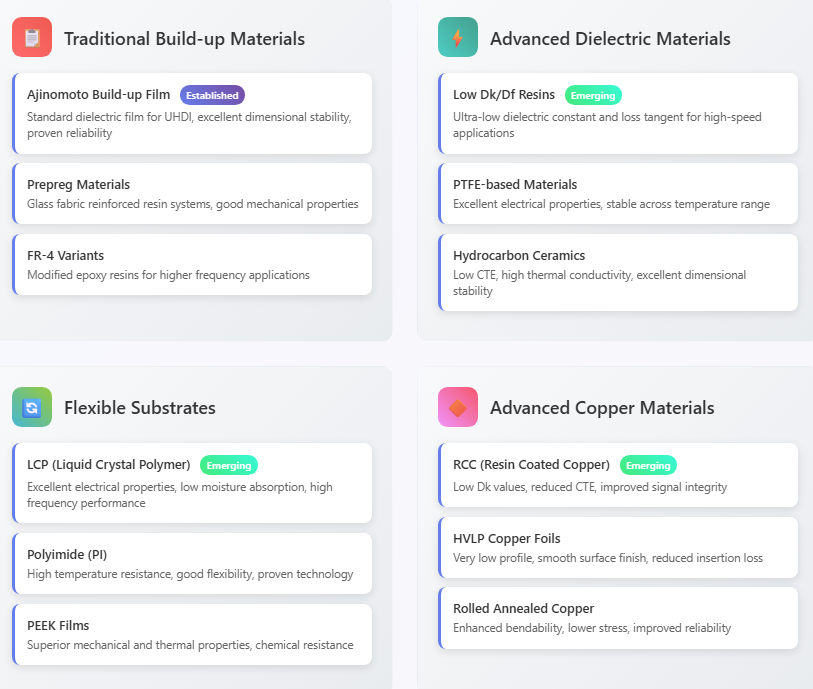
Buildup material options used in a UHDI process for substrate-like PCBs.
UHDI Fabrication Capacity for Substrate-Like PCBs
As density increases, traditional etched copper processing will no longer be useful for substrate-like PCBs, and indeed this is already happening for systems incorporating advanced silicon. The available fabrication and assembly capacity for these components varies with geography. As is typical for most capacity in the PCB industry, the bulk of the world's capacity is located in China and Taiwan. Other countries in Southeast Asia like Singapore and Malaysia also boast fabrication and assembly capacity for these designs. Some Chinese manufacturers actively market substrate-like PCB fabrication capabilities on their websites with the intention of targeting SMBs as potential customers.
In the United States and Europe, the fabrication and assembly capacity for these products is much lower. The capability has also been historically less advanced than what is available in Southeast Asia. However, as of 2025, new investments in UHDI fabrication capacity are changing the capability mix in the United States. Some of the larger fabrication companies are now offering UHDI as a prototyping capability or high-mix/low-volume capability for both substrate-like PCBs and IC substrates.
| Company | Country | Primary Capabilities | Market Focus |
|---|---|---|---|
| Southeast Asia (Advanced Capabilities) | |||
| Unimicron Technology | Taiwan |
High Volume Substrate-like PCB IC Substrates |
Mobile devices, networking, automotive |
| AT&S | China/Korea |
High Volume Substrate-like PCB IC Substrates |
Automotive, industrial, mobile |
| Zhen Ding Technology | Taiwan |
High Volume Substrate-like PCB |
Consumer electronics, mobile |
| Samsung Electro-Mechanics | South Korea |
High Volume IC Substrates |
Mobile processors, memory packages |
| Shinko Electric Industries | Japan |
High Volume IC Substrates |
Advanced packaging, semiconductors |
| Ibiden | Japan |
High Volume IC Substrates |
CPU/GPU substrates, networking |
| Nan Ya PCB | Taiwan |
High Volume Substrate-like PCB |
Networking, servers, automotive |
| United States (Emerging/Expanding) | |||
| TTM Technologies | United States |
Prototyping Substrate-like PCB |
Defense, aerospace, automotive |
| Advanced Circuits | United States |
Prototyping Substrate-like PCB |
Quick-turn, prototyping, low-volume |
| Benchmark Electronics | United States |
Prototyping Low Volume |
Medical, aerospace, industrial |
| Sanmina | United States |
Prototyping Low Volume |
Communications, defense, medical |
| Europe (Developing Capabilities) | |||
| AT&S (Austria) | Austria |
Medium Volume Substrate-like PCB IC Substrates |
Automotive, industrial, mobile |
| Würth Elektronik | Germany |
Prototyping Substrate-like PCB |
Automotive, industrial electronics |
| Printed Electronics Ltd | United Kingdom |
Prototyping Low Volume |
Research, development, specialized applications |
| Elvia PCB Group | France |
Prototyping Substrate-like PCB |
Aerospace, defense, medical |
Looking to the Future With UHDI
Substrate-like PCB as a design approach, UHDI as a fabrication approach, assembly of bumped dies on fine pitch batteries, and the chiplet revolution are all converging to allow new types of designs at lower cost and with more advanced features.
With new fabrication capacity coming into the US and a demand by mil-aero OEMs for higher feature densities in new battlefield systems, we believe more companies in the defense sector will be taking charge of their chip and PCB designs in a comprehensive workflow, which is likely to include the use of substrate-like PCBs.
Whether you're designing ITAR-controlled PCBs for defense systems or EAR-regulated electronics, you need a design partner that understands export control requirements. NWES helps defense contractors and aerospace OEMs navigate complex regulatory frameworks while delivering reliable, manufacturable designs. We've also partnered directly with EDA companies and advanced ITAR-compliant PCB manufacturers, and we'll make sure your next high speed digital system is fully manufacturable at scale. Contact NWES for a consultation.
Ready to start your next design project?
Our Clients and Partners



















