
Most of the products that power our modern lives require electronic components and specialized materials. The electronics supply chain has grown to the point where it can reliably deliver components, materials, and finished products in moderately short time frames, even when customers and vendors are on opposite sides of the globe. While the electronics supply chain is most often associated with electronic components, it actually encompasses a range of materials, equipment, and services that make the supply chain possible. Companies looking to produce a new product, whether at low or high volume, should understand these dynamics, as well as where to procure the materials they need.
In our work with innovative startups and larger companies developing their first suite of electronic products, customers may be in for a rude awakening once they see how the electronics supply chain actually works. This guide provides an overview of the supply chain, especially as it pertains to companies planning to scale into high-volume PCBA manufacturing.
What Goes Into a New Product
All electronic devices rely on semiconductors and PCBs, as well as the materials and processes used to assemble them. The fastest way to understand what goes into a new product is to look at a PCB and all of its components. We created the graphic below to show a breakdown of all the parts of a PCB that go into a new product.
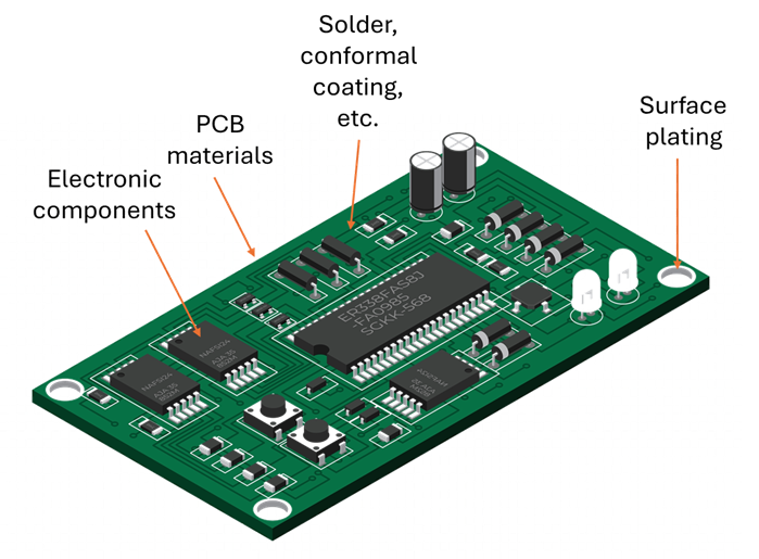
PCB with different parts and materials indicated.
Product designers and engineers play the lead role in specifying each of these components for a new design. The level of specification can vary greatly depending on the product and its performance or reliability needs. Clear designs may require less specification, allowing your PCB manufacturer to fill in the gaps. A contract PCB design firm can also help specify certain points in the design, particularly when customers are not experts in PCB design or manufacturing.
Electronic Components
Electronic components—and most notably semiconductors—are the stars of the show in any electronics assembly. PCBs are designed and engineered specifically to support the manufacturing of interconnects between electronic components while allowing the propagation of signals between them. The electronic component supply chain receives the most attention, and deservedly so; no electronic device would function without components mounted onto a PCB.
The supply chain ecosystem for electronic components follows a simple structure, similar to what is found in other industries. Manufacturers produce components and sell them wholesale to distributors, who then sell smaller lots to electronics designers, contract manufacturers, EMS companies, and prototyping houses. Distributors generally support the low-to-medium-volume production segment of the electronics market, which spans a wide range of devices and industries.
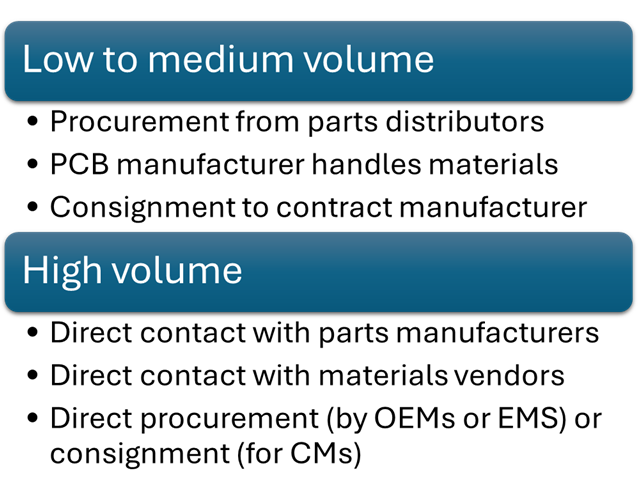
It is also possible to procure components directly from manufacturers, although only some manufacturers sell directly to designers or contract manufacturers at low volume. Some semiconductor companies have their own e-commerce sites, allowing them to sell directly to customers—though typically at prices that match those of distributors.
For high-volume production—generally at volumes exceeding what authorized distributors can supply—companies may need to approach electronic component manufacturers directly for purchases. This requires entry into their sales channels and direct communication with an account manager. Additionally, minimum order quantity (MOQ) requirements must be met when buying directly from component manufacturers. If you're in the sales channel and speaking to the right people, it's possible to secure regular allocations of components directly from the manufacturer, avoiding distributor markups.
PCB Materials Supply Chain
PCB designers who are more familiar with material properties often specify certain materials for use in their assemblies. The most common specification is for PCB laminate materials, but the electronics supply chain includes materials that extend far beyond the dielectric materials used in PCB stackups:
- Copper foils, including electrodeposited and rolled-annealed copper foil types
- Adhesives and encapsulant materials used for bonding and protecting unpackaged semiconductor dies
- Underfill materials for filling voids in BGA packages or bumped dies
- Cleaning chemicals for removing chemical residues and solder residues
- Solder formulations used in PCB assembly
- Conformal coatings, which can act as RF shielding materials and environmental barriers
- Conductive or non-conductive epoxy materials for filling via holes
- Plating chemistry precursors
- Potting materials used in encapsulated assemblies
Some products require a high level of specification for all materials in the PCB and PCBA. This is most often outlined in the master fabrication and assembly drawings.
In terms of supply chain visibility, PCB designers and EMS customers often have little insight into the availability and inventory of these materials. There are no centralized systems compiling supply chain data, so customers must obtain information directly from product manufacturers—if available. This makes it challenging to plan production runs specifically around material availability. Fortunately, many PCB and PCBA materials have suitable substitutes, though some advanced designs require materials that have no readily available alternatives.
PCB Manufacturing Capacity
Another critical consideration in the electronics supply chain is PCB manufacturing capacity. As mentioned above, the majority of high-volume PCB manufacturing is located in Southeast Asia, particularly in China. However, manufacturing capacity is expanding geographically—most notably into India and Latin America—as EMS companies engage in mergers and acquisitions (M&A) and attempt to geographically diversify their supply chain risk. Any company planning to produce a new electronic product must determine where they will manufacture it as part of their budgeting and pricing strategy.
Companies producing in the U.S. or Europe typically find ample prototype capacity and moderate-volume PCB assembly capacity. However, for low-cost, high-volume production, Southeast Asia remains the best option, with the majority of capacity located in China. For some export-controlled products, production will be limited to specific locations, and domestic options may be the only permissible route.
For U.S. companies, production in Canada is also an option under the Joint Certification Program (JCP), though products may require an export license and/or ITAR registration.
When outsourcing PCB design work to a contract design firm, the outsourced firm plays a crucial role in ensuring that designs can be procured at the required volume without excessive lead times or costs. Strategies to mitigate risks include:
- Partnering with a vetted group of manufacturers
- Maintaining direct relationships with material distributors
- Purchasing only from authorized component distributors
These approaches ensure a stable supply chain for overseas production, localized prototyping, and any build volume in between.
Whether you're designing high-speed PCBs for mil-aero embedded systems or a complex RF product, you should work with a design and development firm that can ensure your product will be reliable and manufacturable at scale. NWES helps aerospace OEMs, defense primes, and private companies in multiple industries design modern PCBs and create cutting-edge embedded technology, including power systems for high reliability applications and precision control systems. We've also partnered directly with EDA companies and advanced ITAR-compliant PCB manufacturers, and we'll make sure your design is fully manufacturable at scale. Contact NWES for a consultation.
Ready to start your next design project?
Our Clients and Partners


