

Today's defense electronics companies need to move quickly to bring new products to warfighters. This means cutting down the time between prototyping runs and producing the total number of prototypes during new product development. This isn't just about cost, it's also about time to market and maintaining readiness in a competitive industry. The industry leaders we work with know this to be true, including for printed circuit boards, and yet they still have trouble developing a clear strategy and process for rapid prototyping and eventually beginning LRIP.
In this article, we outline some of the strategies we use to procure circuit boards for electronics equipment, both for aerospace and warfighters on the ground. Working with an experienced PCB design firm that is also a military PCB supplier gives a distinct advantage by eliminating overhead, providing access to multiple capability levels, and ensuring a faster DFM review.
The information in this article does not constitute legal advice and may not apply to every product that ultimately becomes military hardware. Always consult with counsel or procurement experts if you're unsure of your compliance obligations under ITAR/EAR99 as they pertain to your particular product.
Develop Your Intentions First
We have found that defense electronics project schedules can often get stretched endlessly, especially when looking at the PCBA and complex systems. Most often, multiple PCBAs need to interface with each other and all of them will need to be prototyped.
In rapid prototyping, you should try to answer the following question: what do we want to do with these rapid prototypes?
It's an important question because this will determine where you produce, the cost involved, and the lead time you can expect. Depending on the piece of equipment, the IP built into the PCB, and the complexity of the device, there are cases where a low-cost overseas supplier might be appropriate. One prototyping path we have implemented for clients which keeps costs under control and provides short lead times is as follows:
- Develop test PCB prototypes for specific circuits
- Develop functional prototypes, sometimes in multiple spins
- Finalize the design and plan for low rate initial production (LRIP)
While developing a simple test PCB at the beginning of the project with targeted circuitry might seem to be adding excessive time to a schedule, these devices can be rapidly prototyped alongside the functional prototypes in order to allow for circuit configuration and testing. If you can get your important circuitry functioning correctly on a test PCB that will never appear in a built product, you reduce the risk in your functional prototype runs and can even reduce spins, which will save a significant amount of cost. These specialized circuits can be developed early and put into prototype while the PCB design team finishes the complete product design.
Embedded Development and PCB Design in Parallel
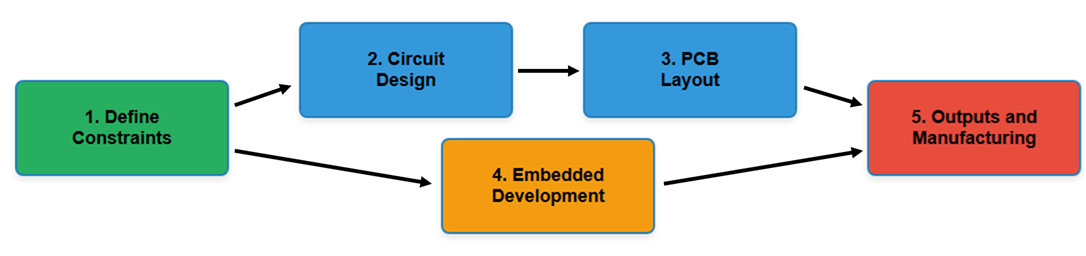
Rapid prototyping eliminates the possibility that development work can be done sequentially. To get to a minimal time frame for completing product design, embedded development work needs to occur in parallel to the PCB design. As is the case with many open standards, legacy systems, and innovative new products, mechanical form factor often drives the design first, especially when we look in areas like aerospace. With the mechanical form factor determined, this sets many of the constraints on the PCB which the designers must stay within.
An example flowchart is listed below outlining the product development steps in sequence. Unfortunately, not everything can be done in parallel, but once the constraints and application goals are defined, the electrical and embedded development can often proceed in tandem.
Embedded development requirements do place some constraints on the electrical design regarding usage of high pin count processors, particularly FPGAs. Specific pins may need to be used for certain interfaces so that subsystems in the design can communicate. The FPGA developer can drive this at the beginning of the design phase, but pin swap lists are always helpful to make the PCB layout easier. Developing these pin swap lists at the beginning of the PCB design phase when placement is being completed will help the PCB designer create a functional layout.
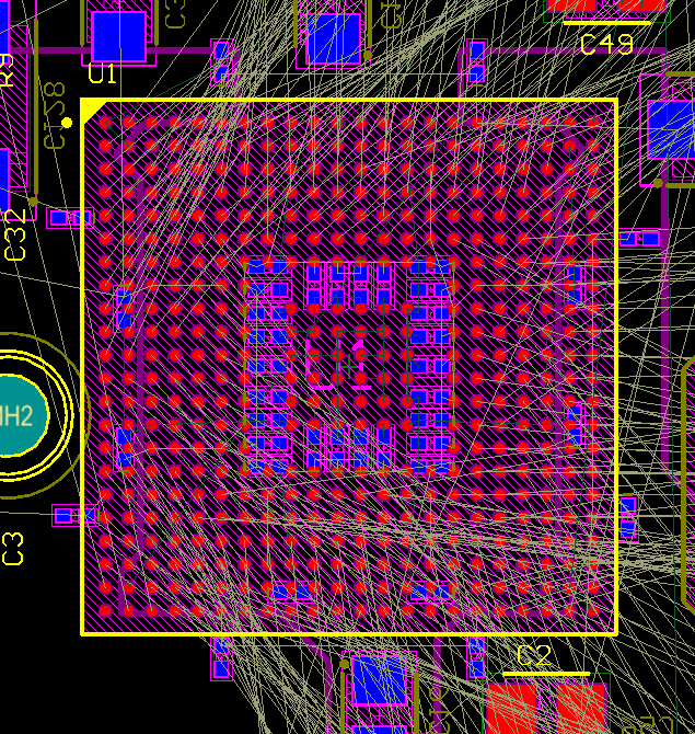
Altium Designer pin swapping interface in the PCB Editor window.
Overseas or Domestic PCBA Manufacturing?
Without question, full production for military electronic equipment should be done domestically in order to comply with ITAR and EAR99 regulations. But in the early prototyping phase, some simple test boards could be produced overseas, and often faster and for lower cost than would be done domestically. Depending on the customer requirements and contract terms, this is an option to explore.
Even if the specific components to be assembled and the IP that will make its way into the application are not covered under ITAR or EAR99, we still advocate that assembly of any PCBs produced overseas be performed in the US. For simple PCBs, including test circuit PCBs, an overseas fabricator will not have any information on the end products, and it is also acceptable to obfuscate the end customer by using a PCB supplier as an intermediary. The real IP often only appears in the CCA once components are assembled onto the PCB. Once ITAR/EAR99 covered components are assembled onto a PCB and an application is running on the PCB, the overseas-produced PCB now becomes an ITAR/EAR99 covered product.
Here is one process we have used to help customers get through rapid prototyping by taking a domestic and overseas strategy:
- A test PCB for specific circuitry is built with an overseas quick-turn PCB fabricator. No IP that would fall under ITAR or EAR99 can be contained in the PCB.
- The completed prototype from the overseas shop is shipped to a domestic ITAR-registered assembler. These assemblers can then handle your ITAR or EAR99 covered electronic components.
- Parts are procured from a US franchise distributor who will handle all the logistics and compliance for ITAR/EAR99 components.
- After test circuit validation, a functional prototype spin can be produced from a rapid prototyping shop in the US.
- Rapid PCB prototypes are consigned to a US assembler and CCAs are provided under a quick-turn service level.
By placing part of the fabrication and assembly work overseas in parallel with the domestic production work, the front-end portion of the design phase can get done quicker and it reduces risk for the intermediate rapid prototyping phase.
Leverage Dev Boards and Modules First
For embedded systems development, dev boards and modules are very useful as they provide working circuitry that allows developers to focus on the embedded application rather than first-pass hardware design. We have seen many companies build their first prototypes for embedded systems without considering the needs of the embedded application or consulting with a developer. Oftentimes, these prototypes end up having so many problems that rework is not possible, and the designs only become useful for partial circuit reuse and reliability testing.
When available, try to leverage development boards, evaluation kits, and even open-source designs for testing the basic circuit functionality and developing an embedded application. These products are available off the shelf from franchise distributors and can be shipped to your facility quickly. Once the basic functionality is qualified, you can proceed to a first prototype spin with greater confidence that your custom PCB will work correctly.
Working With Quick-Turn PCB Shops
There are many quick-turn shops in the US that can produce bare PCBs and assemblies with short lead times. We advocate using these vendors when schedules get compressed and cost becomes less of a concerning factor. While the costs can be significantly higher than manufacturing overseas, the lead time and service level are excellent, and the capabilities accessible locally at quick-turn shops are comparable to those at overseas PCB fabrication facilities.
Some of the types of PCBs one can access at US facilities under a rapid prototyping service level include products from the following list:
- Rigid PCBs in as fast as 24 hours
- Multi-layer flex and rigid-flex PCBs
- Sublimation build PCBs
- HDI PCBs on standard stackups
- RF PCBs on common PTFE materials
- More advanced HDI PCBs like ELIC
More advanced products like UHDI PCB fabrication and substrate-like PCB fabrication are available at low volumes. Currently, these are not typically offered under a quick-turn service model, but we expect that to change going into the future as more investment flows into building these capabilities for mil-aero and commercial products.

When in Doubt, Choose Domestic Production
There are clear advantages to overseas production of military electronics as they relate to rapid prototyping, as well as cost reduction when necessary. But for most products which will end up in military equipment, domestic production is the only compliance option. Domestic production also gives greater assurance that IP will be kept confidential by the manufacturer, many of whom are ITAR-registered manufacturers.
To get access to innovative manufacturers that can help control cost and provide quicker end PCBs under a rapid prototyping model, contact a company like NWES. We provide managed manufacturing through multiple partner sites in the United States and overseas. With our qualified broker network, franchise distributor relationships, and relationships with PCB manufacturers, we can help balance lead time and cost while ensuring clients can access the capabilities they need for advanced builds.
Whether you're designing high-speed PCBs for mil-aero embedded systems or a complex RF product, you should work with a design and development firm that can ensure your product will be reliable and manufacturable at scale. NWES helps aerospace OEMs, defense primes, and private companies in multiple industries design modern PCBs and create cutting-edge embedded technology, including power systems for high reliability applications and precision control systems. We've also partnered directly with EDA companies and advanced ITAR-compliant PCB manufacturers, and we'll make sure your design is fully manufacturable at scale. Contact NWES for a consultation.
Ready to start your next design project?
Our Clients and Partners



















