
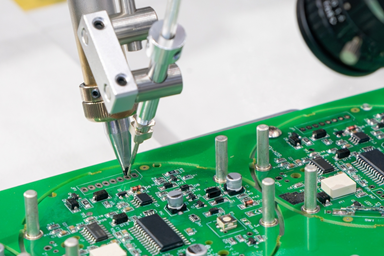
Despite the success of the SMD revolution and the proven reliability of SMD parts, through-hole parts are not going away and PCB designers still need to create footprints for these components. Through-hole parts require a finished hole size that provides some margin between the lead and the internal hole wall so that solder can infiltrate into the through-hole. This ensures a strong connection to the through-hole once the PCB is assembled.
This article gives some easy-to-follow guidelines on sizing holes for through-hole components used in PCBs. These guidelines are based on IPC standards and basic assembly procedures used in PCB manufacturing.
IPC Density Level For Through-Hole Components
The IPC-7251 standard defines three density levels for through-hole component design, similar to what is used in IPC-7351 for SMD components. These density levels are:
- Level A (Maximum), used for low-density PCB assemblies
- Level B (Nominal), used for moderate density PCB assemblies
- Level C (Minimum), used for high density PCB assemblies
The density level is the first place to start determining the appropriate hole size for a through-hole component. When we want to have a higher density assembly, we use smaller holes to try and get some additional margin wherever possible.
the next piece of information we need is the maximum lead diameter for the component in question. The maximum lead diameter is determined from a component datasheet and it can be found in a mechanical drawing. Lead diameters always have a nominal value and tolerance, and the positive tolerance value + nominal lead diameter gives the maximum lead diameter. In some mechanical drawings, a maximum value is given without a tolerance value, and this value can be used directly to calculate the hole diameter.
Minimum Plated-Thru-Hole Diameter and Pad Size
The minimum plated through-hole diameter is the finished hole size, not the drill diameter. This is because the plating thickness in a through-hole can be specified to be larger than standard (>1 mil), depending on the application and reliability expectations. This means that the plating thickness needs to be added to get the drill size. However, for most PCBs produced with standard capabilities, the finished hole size and drill location tolerances will be larger than the nominal plating thickness, so it is often appropriate to use the minimum through-hole size as the drill diameter as there will still be plenty of margin.
To get the minimum hole diameter, we add a factor to the following table based on the target density level from the IPC standards. These are summarized below:
| Density Level | Minimum Hole Diameter |
|---|---|
| A (Maximum) | Hole diameter = Lead diameter + 0.25 mm |
| B (Nominal) | Hole diameter = Lead diameter + 0.20 mm |
| C (Minimum) | Hole diameter = Lead diameter + 0.15 mm |
Next, we need the pad size. The pad size needs to be large enough to ensure sufficient annular ring on the through-hole pad after the PCB is drilled. This is based on them factory’s IPC Producibility Level and the IPC product classification your design needs to meet (Class 2, Class 3, etc.). Most PCB fabrication companies are producing at Level B (moderate precision) or Level C (highest precision). Your PCB fabrication company’s capabilities statement will tell you what level of pad oversize is required for different product classes.
For example, suppose the minimum annular ring for your fabrication house is 0.05 mm. The IPC density level target for the design can be used to determine the pad size by adding another margin factor to the minimum hole diameter:
| Density Level | Minimum Pad Diameter |
|---|---|
| A (Maximum) | Pad diameter = Hole diameter + (0.05 mm + 0.30 mm)x2 |
| B (Nominal) | Pad diameter = Hole diameter + (0.05 mm + 0.25 mm)x2 |
| C (Minimum) | Pad diameter = Hole diameter + (0.05 mm + 0.20 mm)x2 |
Once the pad diameter and minimum hole diameter are determined, the hole can be placed in the PCB layout or in the library component.
Solder-Dipped Through-Hole Components
In aerospace electronics, maximum reliability is a requirement, and that most often requires qualifying components or intentionally buying MIL-SPEC components directly from manufacturers. Unfortunately, not all through-hole parts have a MIL-SPEC variant available, but as long as the lead finish is appropriate (no pure tin), the component leads can be solder dipped to ensure enhanced reliability of the assembled part.
Solder dipping (a.k.a. dip soldering) is exactly as its name suggests: through-hole components or free wires are immersed in a molten solder bath to apply a pre-coating before assembly onto a bare PCB. This method helps to facilitate reliable soldering when non-standard platings are used on component leads. While it is not a requirement for soldering through-hole parts to a design, testing of certain parts may reveal that solder dipping provides higher reliability assembly for through-hole components.

If dip soldering will be used on through-hole parts, an additional allowance on the through-hole diameter in the PCB may be needed. This could also be compensated with thinner plating in the through-hole, but this is not recommended as it will reduce the reliability of the connection. Consider adding an additional 0.05 mm to 0.1 mm diameter on the drill diameter. In some cases, depending on the solder formulation, temperature, and viscosity, no oversize will be needed. A simple test board can be used to check this before a production run.
Once solder dipping is performed, any of the standard soldering processes for through-hole components can be used (hand soldering, selective soldering, wave soldering, or pin-in-paste with reflow soldering). The newly applied molten solder will bond onto the existing dipped solder film and form a strong joint in the through-hole.
Whether you're designing high-speed PCBs for mil-aero embedded systems or a complex RF product, you should work with a design and development firm that can ensure your product will be reliable and manufacturable at scale. NWES helps aerospace OEMs, defense primes, and private companies in multiple industries design modern PCBs and create cutting-edge embedded technology, including power systems for high reliability applications and precision control systems. We've also partnered directly with EDA companies and advanced ITAR-compliant PCB manufacturers, and we'll make sure your design is fully manufacturable at scale. Contact NWES for a consultation.
Ready to start your next design project?
Our Clients and Partners



















