

Electronic systems deployed in extreme environments face challenges that rarely appear in commercial electronics. Military platforms operating underwater or in aerospace environments expose components and assemblies to pressure conditions far outside the range encountered in typical industrial or consumer products. In these environments, pressure becomes a major driver of mechanical stress, material behavior, and long-term reliability.
Understanding how pressure affects electronics requires looking beyond traditional electrical specifications. Component packages, PCB materials, solder joints, and even trapped gases inside assemblies can behave very differently when subjected to high hydrostatic pressure underwater or the near-vacuum conditions encountered in aerospace systems. Engineers designing electronics for these environments must treat pressure as a fundamental design constraint rather than an afterthought.
Pressure as a Mechanical Reliability Driver in Electronics
Pressure affects electronic assemblies primarily through mechanical interactions with materials and internal voids. Electronic components are not solid blocks of material. They contain mold compounds, die attach layers, bond wires, encapsulants, and internal cavities. When pressure changes significantly, these internal structures experience stresses that can degrade reliability over time.
Several mechanisms commonly appear when electronics operate in extreme pressure environments.
Package deformation - Many semiconductor packages are built with epoxy mold compounds surrounding the die and lead frame. These materials have finite stiffness and can deform under mechanical loading. Under high pressure, this deformation can place additional stress on bond wires and die attach interfaces.
Pressure differentials across cavities - Some components contain small internal cavities or trapped gas volumes. Examples include MEMS devices, sensors, oscillators, and certain RF components. Large pressure differences across these cavities can cause structural deformation or permanent damage.
PCB material compression - PCB laminates are composite materials made from glass reinforcement and resin systems. High external pressure can compress the dielectric layers, potentially changing mechanical stress distributions within plated through-holes, vias, and solder joints. This can be addressed with fixation and heat management.
Outgassing and internal pressure buildup - In vacuum environments, volatile compounds trapped in materials can outgas. The removal of external pressure can also cause trapped gases to expand, potentially damaging packages or contaminating nearby sensitive surfaces.
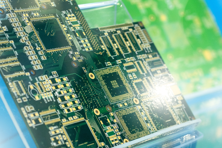
Designing Electronics for High-Pressure Underwater Environments
Underwater electronics appear in a wide range of military and industrial platforms including autonomous underwater vehicles (AUVs), remotely operated vehicles (ROVs), sonar systems, subsea sensor networks, and deep-sea instrumentation. At depth, electronics must withstand substantial hydrostatic pressure.
As a rule of thumb, water pressure increases by approximately 1 atmosphere every 10 meters of depth. A system operating at 1,000 meters depth experiences roughly 100 atmospheres of pressure. At these pressures, mechanical stresses on enclosures and internal electronics become significant.
Pressure Tolerant vs Pressure Vessel Designs
Engineers typically use one of two design strategies for underwater electronics.
| Design Approach | Description | Advantages | Challenges |
|---|---|---|---|
| Pressure Vessel | PCB and components are enclosed in a sealed housing designed to withstand external pressure. | Protects the system from mechanical stress and moisture. | Heavy housings, large mechanical structures, sealing challenges. |
| Pressure Tolerant | Electronics are exposed to external pressure, often immersed in oil or another incompressible fluid. | Smaller enclosures and lighter structures. | Components must survive direct hydrostatic loading. |
Pressure-tolerant electronics are increasingly common in modern underwater systems because they reduce the size and weight of subsea equipment. However, this approach requires careful component and PCB design.
Mechanical Stress on Component Packages
When electronics are directly exposed to hydrostatic pressure, the load is transmitted through the surrounding fluid and applied to the surfaces of components and PCB assemblies. Several component types require special attention, including plastic encapsulated semiconductors, ceramic packages, MEMS sensors, oscillators and resonators, and electrolytic capacitors.
Plastic molded packages may compress slightly under pressure, which can stress bond wires or die attach layers. Ceramic packages are generally more rigid but may transfer higher stress into solder joints. MEMS devices are particularly sensitive because many rely on microscopic mechanical structures that can be affected by external pressure.
PCB Structural Considerations
Under high hydrostatic pressure, the PCB itself experiences compression. Although the absolute dimensional change may be small, the resulting stress can affect several structures within the board stackup and assembly.
- Via barrels and plated through-holes
- BGA solder joints
- Large components with stiff packages
In pressure-tolerant systems, engineers often reduce these risks through smaller component packages, reduced component height, even distribution of mechanical loads, and increased board thickness for structural rigidity.
Fluid Compatibility and Contamination Control
One approach to implementing pressure-tolerant electronics is to immerse the PCB assembly in an insulating oil or other incompressible fluid. The fluid transmits pressure evenly while its sealing to the enclosure prevents water ingress.
However, immersion introduces additional reliability concerns. Fluid absorption into polymers, long-term compatibility with plastics and elastomers, and chemical contamination of components must all be evaluated during the design process. Engineers typically verify that component materials and PCB finishes remain stable in the chosen fluid over the expected operational lifetime of the system.
Designing Electronics for Low-Pressure Aerospace Environments
At the opposite extreme from deep-sea systems, aerospace electronics must operate in low-pressure or near-vacuum environments. These conditions are common in high-altitude aircraft, spacecraft, satellites, and vacuum instrumentation. Although the absence of pressure may appear less mechanically demanding than deep-sea conditions, vacuum environments introduce their own set of reliability challenges.
Outgassing in Vacuum Systems
One of the most important reliability concerns in vacuum electronics is outgassing. Many materials used in electronics manufacturing contain volatile compounds that can evaporate when exposed to vacuum.
- Epoxy resins
- Adhesives
- Potting compounds
- Conformal coatings
- Certain PCB laminates
In vacuum environments, these materials can release gases that migrate and deposit onto nearby surfaces. This is particularly problematic in aerospace systems containing optical sensors, laser systems, imaging instruments, and RF or microwave hardware. Deposited films can degrade optical performance or interfere with sensitive electronic components.
To mitigate these risks, aerospace programs often require materials that meet NASA outgassing standards, typically defined by Total Mass Loss (TML) and Collected Volatile Condensable Materials (CVCM). Engineers should verify that PCB materials, coatings, and adhesives comply with these limits before integrating them into vacuum systems.
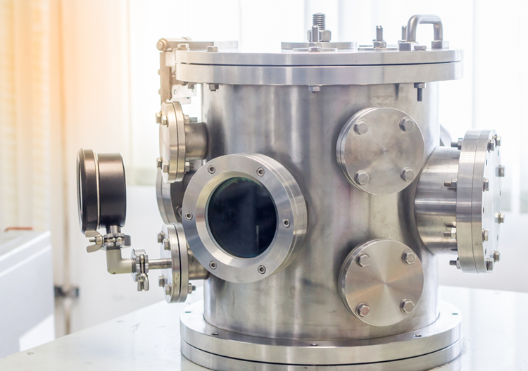
High and low pressure conductions can be simulated in small environmental chambers.
Internal Pressure in Component Packages
Many electronic components contain sealed internal volumes filled with air or inert gases. Examples include:
- Crystal oscillators
- MEMS sensors
- Certain RF filters
- Hermetic packages
When these components are exposed to vacuum, the pressure differential between the internal cavity and the external environment can place mechanical stress on package structures.
In most commercial components this pressure difference is small enough to tolerate, but in extreme environments engineers should confirm the pressure rating of sensitive components.
Thermal Behavior in Vacuum
Pressure also affects how electronics dissipate heat. In terrestrial environments, convection contributes significantly to heat removal. In vacuum conditions, convection is essentially eliminated. Heat transfer must therefore occur through:
- Conduction through the PCB and structure
- Radiation to surrounding surfaces
This change in thermal behavior can increase the operating temperature of components, which indirectly affects reliability. Design techniques commonly used in aerospace electronics include thermal conduction paths through metal structures, heat spreaders integrated into PCB stacks, and controlled component placement near thermal interfaces.
Reliability Testing for Pressure-Sensitive Systems
Whether designing for subsea or aerospace applications, component selection becomes a key part of reliability engineering. Design teams typically evaluate components using the following criteria:
- Package type
- Internal cavity structures
- Mechanical robustness
- Material compatibility
Note that hermetic ceramic packages generally offer better environmental resistance than plastic molded packages, although they come with higher cost and larger size. MEMS devices, oscillators, and pressure-sensitive sensors require special evaluation when exposed to large pressure changes. Packages with large die areas or long bond wires may also be more susceptible to mechanical stress. In addition, encapsulants, adhesives, and PCB laminates must be compatible with immersion fluids or vacuum environments depending on the application.
Pressure sensitive systems demand laboratory testing to ensure they can withstand pressure demands in the field. Typical test methods include hydrostatic pressure testing for subsea electronics, vacuum chamber testing for aerospace electronics, thermal-vacuum cycling to simulate orbital environments, and pressure cycling tests to evaluate long-term fatigue effects. These tests allow engineers to identify failure mechanisms early in development and refine the mechanical design of the system. Testing is particularly important for mixed-technology assemblies that include SMD components, MEMS sensors, RF components, and custom PCBs, where pressure-induced stresses may not be obvious from datasheets alone.
Whether you're designing high-speed PCBs for mil-aero embedded systems or a complex RF product, you should work with a design and development firm that can ensure your product will be reliable and manufacturable at scale. NWES helps aerospace OEMs, defense primes, and private companies in multiple industries design modern PCBs and create cutting-edge embedded technology, including power systems for high reliability applications and precision control systems. We've also partnered directly with EDA companies and advanced ITAR-compliant PCB manufacturers, and we'll make sure your design is fully manufacturable at scale. Contact NWES for a consultation.
Ready to start your next design project?
Our Clients and Partners



















