Amplifier Stability: The Complete Design and Analysis Guide
By ZM Peterson • Jan 14, 2021Amplifier design and layout can get much more complicated than component datasheets would have you believe. Anytime an amplifier is designed in terms of circuit design, physical layout, and PCB layout, amplifier stability should be an important consideration. There are times, however, when an amplifier is pushed to its limit and does not exhibit desired behavior, leading to signal distortion on the output.
If you need to layout an amplifier in your PCB, you’re designing an amplifier IC, or you’re designing a front-end from discrete components, pay attention to the different aspects of your design that can create instabilities during operation. Accounting for these points early may help you prevent a failed board spin, power integrity problems, and signal integrity problems during operation.
What is Amplifier Stability?
When we say that an amplifier can be "unstable", we’re referring to how the amplifier transitions away from its initial state when the input signal changes. We’re also referring to the transient behavior, meaning how the amplifier settles into its steady state. There is an entire field of mathematics dedicated to understanding and describing stability in dynamical systems, known as stability theory (unsurprisingly). For amplifiers, we generally only worry about stability in the linear regime as this is where we normally operate with analog signals, even with high power RF signals. For power amplifiers operating with high DC bias, we still have to worry about stability, but in the nonlinear regime, where saturation can occur at high input bias.
Without getting too deep into the mathematics of linear and nonlinear stability analysis, I’ll do my best to outline some important unstable, semi-stable, and limit cycle behavior that can be observed in amplifiers. Here are the principle amplifier stability problems one can observe in practical amplifier circuits:
- Ringing (overshoot/undershoot). Here we have a limit cycle effect, where the output can exhibit a damped oscillation and eventually settle at a stable output.
- Oscillations. This arises due to the impedances of the amplifier output and the load input, which creates a pole in the amplifier transfer function. Although this is a stable effect, it creates bandpass behavior when there should be low pass behavior.
- Parasitic feedback. This is a parasitic coupling effect that creates additional positive or negative feedback to one terminal of an amplifier input. This purely unstable dynamical behavior is best understood in terms of an op-amp circuit, but it can apply in any amplifier.
The importance of amplifier stability really becomes apparent when looking at RF systems, such as telecom systems operating at RF frequencies. These systems use RF power amplifiers that operate with high signal strength and at high frequencies, so their placement in the signal chain must be considered carefully. If there is a layout mistake or undesired parasitics in the layout, you’ll observe undesired instabilities in the output signal. RF power systems should always be tested for unstable behavior throughout the desired power range to ensure the system will operate as designed.
If you’re interested in understanding linear and nonlinear stability in dynamical systems, there are many textbooks on the topic that can help you get started. I suggest tutorials on the Poincare`-Bendixson theorem. Otherwise, keep reading to learn more about what governs amplifier stability in real circuits.
What Causes Amplifier Instability
There are three points mentioned above, and most electronics designers don’t concern themselves with these various areas of instability in electronics. Let’s look at each of the three effects to see what aspects of an amplifier circuit, the load impedance, and the PCB layout govern amplifier stability. I’ll discuss these points in terms of an op-amp as this provides a simple reference for understanding amplifier stability generally.
Transient Ringing
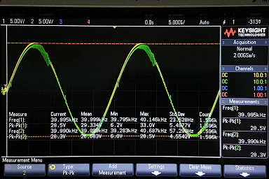
Ringing is a transient effect, just like you might see in any other circuit when it is switched between two DC levels. The transient response from an amplifier can appear the same as the transient response in any other circuit, but it should not be confused with the typical ringing effects in transmission lines (repeated reflections, ground bounce, or resonance on short lines. This is shown in the graph below.

Ringing is a limit cycle behavior that indicates amplifier stability.
Ringing arises because there is some capacitance in the amplifier circuit from the load, the feedline between the amplifier and the load, and the amplifier inputs. The feedback loop will interact with the input capacitance, while the amplifier output impedance will interact with both capacitances. The various stray capacitances are shown in the circuit below.

The stray capacitances in this amplifier circuit are highlighted in green. The load has its own capacitance that also affects amplifier stability. Note that there is also some stray capacitance back to the non-inverting input terminal in the above circuit diagram.
The output impedance has some inductance, which is responsible for creating the inductive response required to produce ringing. In other words, the output impedance and the load capacitance in the amplifier form a series RLC circuit, which can have an underdamped resonant response if the output inductance is large enough and the input capacitance is small enough. We can draw the same type of voltage loop back to the stray capacitance on the input terminal. The solutions you use to compensate for ringing are the same as those used to compensate for oscillations, so let’s look at oscillations next.
Oscillations
There’s also the possibility that, when driven with an oscillating waveform, there are strong oscillations observed in the amplifier’s output. This can occur regardless of whether the transient response is overdamped or underdamped, although an overdamped transient response will have much weaker driven oscillation. The problem of oscillations is one of phase margin between the input and output due to feedback.
The interaction between the load capacitance and the feedback network can be understand as a modification of the open-loop gain, which is related to the phase margin. The closed-loop gain is modified from the open-loop gain based on the values of the feedback resistors and load capacitance as follows:
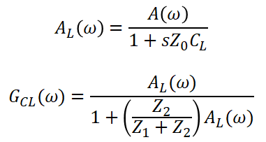
Modification of closed-loop gain due to load capacitance.
As we can see, there is now a pole in the gain spectrum due to the load capacitance, which will have some associated transient response and possible resonance (if the transient is underdamped). If the pole has a positive real part, then we have a growing unstable oscillation. We can derive a similar modification that uses the feedback gain and input capacitance to include a second pole, giving yet another transient response. Some solutions to deal with these oscillations and transient ringing are:
- Adding a series resistor on the output to increase damping (out-of-the-loop compensation)
- For rail-to-rail amplifiers, shunt the oscillation to ground with a snubber circuit (series RC circuit)
- Add parallel capacitance to the feedback loop. This will apply some phase shift to ensure the phase margin is 180 degrees when gain is less than 1.
Parasitic Feedback
This problem arises at high frequencies and is dominated by parasitic capacitance between the amplifier output and input. In effect, this creates an unintended feedback loop back to the amplifier input. The amplifier output has some parasitic capacitance to ground, which is in parallel with the amplifier’s parasitic input capacitance. This creates a low impedance closed loop between the output and input via the ground plane. This can occur at ~GHz frequencies and requires placing isolation between the input and output ports on the PCB. Using vias is sufficient up to ~10 GHz, but problems at higher frequencies require something like shielding on the input line as a coplanar arrangement, or use of electronic bandgap structures (EBGs) between the output and input.

This field solver result shows how the output signal from an amplifier can couple back to an input and produce an oscillation at high frequencies (3.4 GHz shown above). If we had strong coupling back to the non-inverting input, it’s possible for latching to occur when the non-inverting input is driven low. [Source: Keysight]
Comprehensive Amplifier Stability with the K-factor
There is a single metric in amplifier stability analysis that can tell you whether or not your amplifier is stable. This is Rollet’s K-factor, originally published in Stability and Power-Gain Invariants of Linear Twoports (IEEE, 1962). This metric treats your amplifier circuit as a 2-port network. If you can determine the S-parameters for your amplifier circuit, then you can use these to determine the K-factor with the following equation:

Definition of Rollet’s K-factor defining amplifier stability.
Whenever K > 1, the amplifier will always be stable. Otherwise, the amplifier is not guaranteed to be unconditionally stable, and more investigation should be done. This equation is always valid when the amplifier is operating in the linear range and nicely accounts for broadband behavior. Near the amplifier’s saturation point, the S-parameters are only valid if determined using small-signal analysis; this would apply for a small AC signal with large DC offset. For power amplifiers running near saturation, you would use the less-known X-parameters to describe nonlinear amplifier stability.
At NWES, we provide PCB design and layout services to SMBs, large enterprises, and aerospace and defense electronics companies. We know how to deal with amplifier stability, high frequency parasitics, and major signal integrity problems in advanced RF systems, high speed backplanes, power systems, IoT devices, and much more. We’ve also partnered directly with EDA companies and multiple ITAR PCB manufacturing firms, and we help our clients get through the PCB manufacturing process with ease. Contact NWES for a consultation.
Ready to start your next design project?
Our Clients and Partners


