Your Partner in Innovation
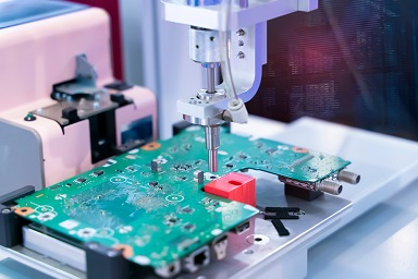
Northwest Engineering Solutions is best known as a PCB design company, but we regularly place client designs into production with on-shore, near-shore, and overseas manufacturing partners. As part of our commitment to providing value to clients, we provide end-to-end management and procurement services throughout the PCB fabrication and assembly process. Whether you need a single prototype or you’re scaling to thousands of units, we’ll work with you throughout the product development process and help you get to market.
If you’re planning to produce your next design as a prototype or at scale, we’ll advise you throughout the process. Our manufacturing partners give us the ability to be agile and find the best solution that fits your production volume, lead time, budget, and design complexity. We work with you to match your design requirements with our manufacturing partner capabilities while considering your budget, required lead time, supply chain and procurement strategy, and regulatory requirements.
A Comprehensive Process
We work with our PCB manufacturing partners to find the right pricing, capacity, capabilities, lead time, and qualification services for your product. Once your new design has passed review and is ready for production, we’ll engage with our manufacturing partners to get your design through production and bring you the most value:
- Engage with us early - We’ll create your new design and develop a strategy to get it manufactured at the required volume. We work to ensure manufacturability at all stages of the design and production process.
- Comprehensive DFM review - We put your design through our review process and identify required changes early. We also work with manufacturers to ensure your design can be put into their PCB fabrication/assembly processes to ensure high quality and yield.
- End-to-end management - We can provide turnkey PCB design and manufacturing services. We'll gather quotes from our partners and work to find the best balance between price, lead time, and capabilities. We work with our partners throughout the process to ensure your production run is on-time and defect-free.
- Certification - We’ll work with our partners to get your build certified under UL, FCC, CE, AS9100, or MIL-STD. We can provide additional testing in-house as needed before shipping finished products to you.
- Compliance - Our experience in mil-aero and our network of ITAR-compliant PCB manufacturing partners makes us an ideal partner for turnkey aerospace and defense electronics design and manufacturing.
Application Areas
For first run prototypes, we provide low-touch full turnkey PCB manufacturing through our partner network. Boards are designed to a standard stackup and process to minimize manufacturing lead time and ensure quality with hassle-free management.
- Standard stackups - Material sets from Isola, ITEQ, or equivalent with low-Tg or high-Tg options with moderate layer counts (up to 12-16)
- Fine capabilities - Fine-line traces, spacing, and drill sizes with high yield and competitive cost
- Thorough evaluation - DFM/DFA review is performed before taking the design to production, customize your testing and inspection requirements
- Scale to volume - Make a seamless transition to high volume production through our larger manufacturing partners

RF PCBs take a different design approach wit specialized material sets. High frequency designs are transitioning away from mil-aero and are appearing in more common devices, such as IoT products that interface with mobile networks. Leverage our experience to make your RF PCB design a reality:
- Dielectrics - PTFE or low-loss FR4 laminates kept in stock in our network, RO4350+RO4450 available for mil-aero PCB builds
- Surface finishes - Standard options for moderate loss dielectrics, we recommend immersion Ag or OSP
- Copper - Available copper materials depend on material system, our partners offer ultra-low profiles if needed
- Exposed plating - Edge and surface plating applied in standard processing for reliable enclosure connections and shielding

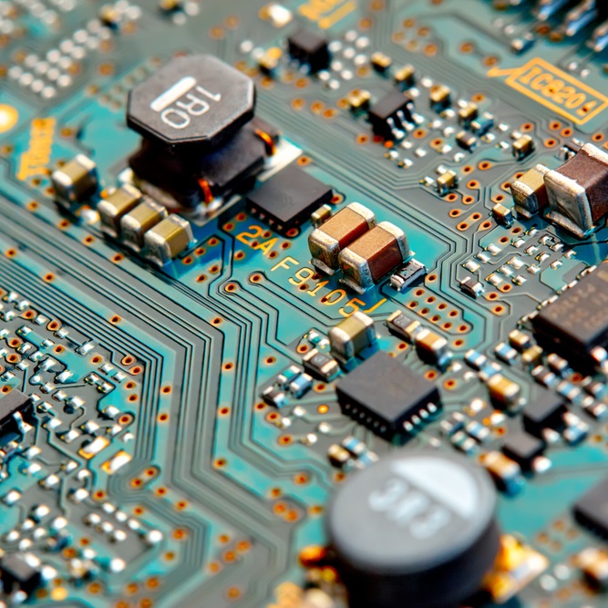
Modern digital systems are packing huge levels of feature density into small packages. Typical applications have been small digital boards with large processors and multiple peripherals, but more specialized areas like medical and commercial space are now using HDI designs. We provide comprehensive in-house design services for advanced high density PCB designs and production support through our partner network:
- Stackups - 1+N+1, 2+N+2/i+N+i, and ELIC HDI PCB stackup options up to 32 layers
- Via options - Through-hole, buried, laser drilled microvias down to 2 mil diameter
- Via fill - Solder mask plug/tenting, conducutive or non-conductive epoxy
- Materials - Stadnard dielectrics compatible with build-up laminations

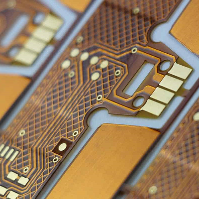
Flex and rigid-flex PCBs provide many opportunities for high-speed and high-frequency systems in tight spaces where reliability is required, such as in mobile devices, military IoT, medical devices, and much more. Our PCB manufacturing partners offer advanced fabrication capabilities for polyimide flex PCBs with or without stiffeners.
- Flex layer stacks - Dual-layer or multilayer flex and rigid-flex assemblies with advanced materials
- Flex fabricationa and assembly - Flex circuit fabrication and assembly capabilities with through-hole and SMD components
- High-speed designs on flex - PCB fabrication supporting high-speed designs with aggressive fill factors and form factors
Designs built to have maximum lifetime and quality must satisfy some of the strictest reliability standards, such as IPC-6012DS. Typical applications are in aerospace and defense electronics, some automotive products, and medical devices. We support modernization and digitization efforts with our turnkey PCB production services for advanced high-reliability desings:
- Rugged assembly - Leaded soldering, mixed through-hole and SMD, automated and manual conformal coating adhesives, encapsulants, and epoxy bonding
- Certification - Facilities certified to AS9100D to support high reliability requirements markets, plus other certifications as required
- Qualification - IPC-A-600 or IPC-6012 inspection levels available, plus additional documentation upon request

Sourcing and Procurement
In times of supply chain volatility, we know how important a sourcing strategy can be to your success. As part of managed PCB manufacturing, we implement a sourcing strategy to prevent delays that can derail your project.
- BOM cleaning and optimization - We’ll go through your BOM to identify and replace obsolete or out-of-stock components. In many cases, we can recommend alternative drop-in replacements that don’t increase the price of your build and incur minimal design changes. For more extensive changes involving critical parts, we can update the design with current parts, and we can accommodate multiple variants as needed.
- Component sourcing strategy - We handle procurement for projects with multiple distributors and design variants. We get started early to ensure your components are in-stock and we procure critical components early when necessary. When parts are out-of-stock from major distributors, we can engage with parts brokers as needed or work to update your design with replacements.
Read our supply chain study to see how we navigate volatility
Related Resources
Who Can You Trust to Source Components for Your PCB Assembly Run?
By A Mughees • Aug 6, 2024Should your PCB assembly house source components in turnkey PCB assembly?
What is Acceptable Attrition in PCB Assembly?
By ZM Peterson • Jun 14, 2024Learn how to manage component overage in PCB assembly, including handling attrition, reasonable loss levels, and factors affecting overage requirements.
PCB Manufacturing Capabilities
Our network of PCB fabrication and assembly partners gives us access to diverse capabilities and lets us approach a range of designs:- Standard processing down to 8 mil clearances/5 mil features with 1 mil tolerances
- Advanced processing down to 3-4 mil clearances/3 mil features with less than 1 mil tolerances
- Controlled impedance design and verification
- Any plating option with conformal coatings available
- High frequency boards with non-standard stackups (e.g., Rogers, Megtron, etc.)
- High layer count HDI PCBs up to 32 layers with laser drilling
- Specialty designs like ceramic PCBs, metal-core PCBs, or hybrid stackup PCBs
- Advanced designs with aggressive form factors that push the limits of signal and power integrity.
Unsure what capability and inspection levels you need? Contact us to learn more or submit your board for quote.
Why Use NWES for PCB Manufacturing?
- Compliant partners - All our PCB manufacturing partners are ISO-9001, AS9100, ISO-13485, IPC-A-610, NADCAP, and/or ITAR/JCP certified.
- Procurement - We’ll manage procurement from major distributors or brokers as needed. We can also modify a design with substitutes when needed.
- Testing and flashing - We’ll specify PCB testing requirements for your build and work with manufacturers to implement on-the-line flashing for your PCBAs.

Contact us today to request a quote and start your next PCB manufacturing project.
Contact us today for more information.
Our Clients and Partners


