
Sequential Lamination and Plating in HDI PCB Manufacturing
By ZM Peterson • Jun 18, 2024See how sequential lamination and plating processes in HDI PCB manufacturing impact HDI PCB designs with high layer counts and reliable interconnects.
Today's electronics have followed the same trend as Moore's Law: more technology and features are being packed into smaller spaces to realize advanced applications. High density interconnect (HDI) PCB design techniques are used to create and layout these advanced assemblies with high component and routing densities, as well as very high layer counts.
At NWES, we help clients push the limits of their designs to the cutting-edge with industry-standard HDI PCB design techniques. We help innovative startups and large enterprise create and qualify their HDI designs, as well as aid the transition from concept to full-scale HDI PCB manufacturing. We look forward to working with you!
Large-scale integration in HDI PCB layout involves multiple low-speed and high-speed digital protocols, as well as a cleear focus on best DFM practices to ensure high-yield production. We adopt a production-first mindset when floorplanning your design, and we'll ensure your high-density PCB layout meets the needs of advanced applications.


![]()
![]()
HDI PCB designs carry important material requirements and component selection considerations that are not found in many other systems. Once your new design has passed review and is ready for production, we’ll engage with our manufacturing partners to get your design through production and bring you the most value:
HDI design starts with a manufacturable stackup that can meet your routing needs, as well as your impedance and loss targets. Standard HDI stackups with via/microvia placement and layer access capabilities are shown below.
| HDI Stackup Type | Via Style |
|---|---|
| Type-I | 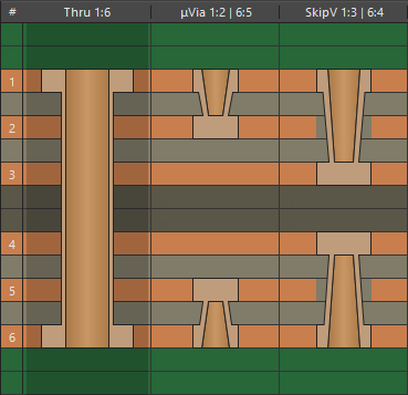 |
| Type-II |  |
| Type-III |  |
| ELIC | 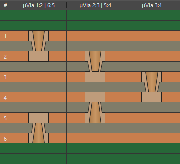 |

As interconnect densities continue to increase, designers must take an ultra-HDI approach that enables innovative electronics packaging, including substrate-like PCBs and advanced substrates for integrated circuits.
Our design expertise is critical to helping clients operate at the cutting edge of technology. Some of the application areas where we operate include:
Our goal is to successfully transition you from concept to product with a fully manufacturable design that can be produced anywhere. Our network of manufacturing partners can help you produce HDI PCB assemblies at scale while staying compliant, sourcing efficiently, and ensuring high yield.
See how sequential lamination and plating processes in HDI PCB manufacturing impact HDI PCB designs with high layer counts and reliable interconnects.

Chrys Shea and Zachariah Peterson discuss SMD tombstoning and evaluation in UHDI PCB assembly.
Read our guide to sizing and use microvias in at low aspect ratio in HDI PCB design, layout, and routing.


