
Guide to PCB Trace Length Matching in High Speed Design
By ZM Peterson • Apr 8, 2020Every electronic signal takes a certain amount of time to travel along a conductor and reach its destination. Due to dispersion and losses in your board, PCB trace length matching in high speed boards needs to be enforced in certain situations. When you know how to identify the sections of a board that require length matching, you can take important steps to ensure your signals arrive at a receiver on time.
If the link between signal velocity and any trace length mismatch is not obvious, the allowed trace mismatch can be determined as a time difference (for digital signals) or a phase difference (for analog signals). PCB trace length matching is normally discussed in terms of differential pairs, but it also applies to nets and buses with single-ended signals and differentially-driven buses. As computer peripherals and other digital systems require successively faster operating speeds, the propagation delay in a computer network places tight tolerances on the allowed trace length in a conductor carrying digital signals. Here are some best practices for applying PCB trace length matching in different types of systems.
Table of Contents
- What is Trace Length Matching?
- Skew and Trace Length Matching
- Clock Signals
- Length Tuning Structures
- What About Analog Differential Signals?
What is Trace Length Matching?
PCB trace length matching is exactly as its name suggests: you are matching the lengths of two or more PCB traces as they are routed across a board. These traces could be one of the following:
- Multiple single-ended traces routed in parallel
- Each end of a differential pair
- Multiple differential pairs routed in parallel
- Single-ended or differential pairs routed in parallel with a clock signal
PCB traces carrying digital signals do not need to be perfectly length matched. There will always be some amount of jitter on the rising edge, so signals routed in parallel can never be perfectly length matched. The goal is to reduce the length or timing mismatch below some limiting value. The allowed length mismatch and timing mismatch are related by the signal velocity:

Relationship between length mismatch and timing mismatch.
If you don’t know the allowed trace length mismatch in your system, don’t fret. Just check your signaling standard, interface standard, or component datasheet. With so much standardization of computer peripherals, most components use one of many high-speed signaling standards, and you can easily find the routing specifications, required impedance, and allowed length mismatch in the specs.
A length mismatch can also be converted to a timing mismatch using the signal velocity (see above), although be extremely careful when selecting the velocity of a digital signal. This is because modern digital signals, generally running with edge rates much less than 1 ns, will have bandwidths reaching into the high GHz and will only tolerate very small mismatches. Dispersion in the PCB substrate causes the signal velocity to vary with frequency. For example, FR4 exhibits normal dispersion below ~1 GHz, so lower frequencies will arrive at the receiver earlier than higher frequencies.
The goal in trace length matching is to prevent skew on a parallel data bus. Skew simply refers to a timing mismatch between the rising edges of two or more digital signals (see below). In a parallel bus, the signal propagating on the shortest trace will arrive earliest, so it will trigger a downstream gate before the other signals on the bus. Industry-standard PCB design software will allow you to define buses and differential pairs in your schematic, but you’ll need to enforce trace length matching in your layout to bring skew within allowed limits.
Skew and Trace Length Matching
Length matching in multiple single-ended nets is rather simple; just add tuning structures to ensure all traces on the bus are the same length. Tuning structures will be discussed in more detail below. For differential pairs, each end of an individual differential pair should be length matched. The diagram below shows an example where PCB trace length matching would be applied to differential pairs.

A driver sending signals down two differential pairs to two different receivers.
The differential pairs shown above are routed between a single driver (e.g., an FPGA) and two different receivers. The receivers each read the differential signals on D1 and D2, respectively. Here, each end of differential pair D1 would need to be length matched. Similarly, each end of differential pair D2 would need to be length matched. However, D1 and D2 do not need to be matched with each other as they are not carrying data parallel. Each of these differential pairs transfers a single bit at a time, and we only need to length-match to ensure common-mode noise is cancelled in each pair.
If you have multiple differential pairs carrying parallel data, each differential pair needs to be matched, and the pairs then need to be matched to each other. This is shown below, where a single driver is sending parallel data to a single receiver. This ensures each differential pair can sufficiently cancel common-mode noise, and it ensures parallel data will be received without skew between bits.
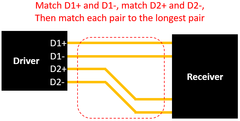
Example of a driver with 2 differential pairs driving a single receiver. All traces should be matched to the longest differential pair.
Clock Signals
The natural next question to ask relates to clock signals: how should signals from a system clock be length matched throughout a digital system with multiple daisy-chained ICs? In the example above, a clock signal needs to come from somewhere in order for the receivers to latch. The answer is: system clock signals aren’t used in this topology!
Using a system clock to trigger every IC in a chain of components is extremely difficult in large digital systems. This is because each IC can have different logic gate delay, rise time, and overall signaling standard. For this reason, modern digital components use source-synchronous clocking or embedded clocking. In the former, a clock signal is routed in a trace alongside the parallel data traces, and this clock trace needs to be length-matched to the other data traces.

Example of a driver with 3 outputs and source-synchronous clocking. All traces should be matched to the longest trace in the bus.
In the case of embedded clocking, there is no clock trace. Embedded clocking is used in serial communication (e.g., SerDes channels) Instead, the clock signal is encoded as the first few bits in the serial data stream. If you’re designing a SerDes channel with differential pairs (e.g., LVDS), the differential pairs still need to be length matched using the techniques shown above.
Length Tuning Structures
There are three common PCB trace length tuning structures, each of which could be discussed in its own article. These are accordion, trombone, and sawtooth tuning. Some other names for these structures are switchback routing and serpentine routing. Each of these different structures can have some interesting effects on transmission line impedance and FEXT, which I’ve discussed in one of my articles on Altium’s PCB Design Blog.
If you’re looking to length match groups of differential pairs, each of these is a good option to lengthen a differential pair. Anytime these structures are applied, you should try to keep the length tuning section symmetric, although Ben Jordan has shown that common-mode noise will still be sufficiently cancelled if the structures lack symmetry.
When escaping a via or if a length mismatch is very short, you should try to apply one of these structures to the source end of the net, rather than at the receiver end. If you apply the structure at the receiver end, any common-mode noise received earlier in the trace may not be sufficiently canceled. For short mismatches near a via, a small delay can be applied at the source end (called phase matching). This is shown on the vias in the above image.

PCB trace length matching when escaping a via.
Signal Integrity Problems From Length Tuning
Length tuning is important for ensuring a differential interface, whether serial or parallel, will function as intended. This is because all differential receivers are crossing detectors and require that the edge rates in the two sides of the signal are crossing each other at the same instant. For a parallel single-ended bus, length matching is only needed within some setup-and-hold time such that logic states are latched within some window defined by the clock.
In differential pairs, length tuning is needed to keep signals synchronized within some timing mismatch limit, but it also creates two SI problems. The first is a small amount of reflection as there is a small impedance mismatch right at the inptu side of the length tuning section. This will become more apparent at higher frequencies when the electrical length of the tuning region becomes long. As a result we have two guidelines for applying length tuning structures:
- The span of length tuning sections should be limited in total length; this will minimize the input impedance deviation at the input of the tuning section.
- Length tuning sections should only be applied in the region where traces in a pair become misaligned, this helps ensure the tuning section is as short as possible.
The reason this impedance mismatch arises is because there can be an odd-mode impedance deviation in the length tuning region, so there is a slight input impedance mismatch looking into the tuning section (read more about differential impedance matching here). The below image shows an example in for a long tuning section, where the characteristic impedance (and thus the odd-mode impedance) experiences deviation in the region where the tuning section is applied.

Impedance deviation resulting from length tuning sections. Read more about this in my article on the Altium blog.
The other signal integrity problem created by length tuning structures is modre conversion. In any differential pair, mode conversion will arise when there is an asymmetry along the routing path, and a length tuning structure is an asymmetry by definition. The problem with mode conversion is that some differential mode signal will be converted to common-mode signal. When there is excessive common-mode power on the output, it can radiate strongly if the signal is passed to an unshielded cable. EMC regulations limit the amount of allowable emissions and common-mode currents being passed from an electronic device and onto a cable.
Mode conversion works both ways, meaning common-mode noise that existed before the length tuning structure was encountered can then be converted to differential-mode noise. This is bad because differential receviers cannot suppress differential-mode noise below the Nyquist sampling limit. Filtering is unacceptable here because it will also filter the signal, causing the device to not work properly. To solve both problems, there is sometimes some additional deskew section added to a differential interconnect to bring the higher frequency components back into phase up to the bitstream's Nyquist frequency. This requires a channel simulation that cannot be performed easily in SPICE, and instead requires a field solver approach with an extracted linear model for the differential interconnect.
At NWES, we’ve built plenty of high speed designs and we know how to get the most out of industry-standard EDA software. We work with electronics companies to design modern PCBs and create cutting-edge technology. We've also partnered directly with EDA companies and several advanced PCB manufacturers, and we'll make sure your next layout is fully manufacturable at scale. Contact NWES for a consultation.
Ready to start your next design project?
Our Clients and Partners


