Flex PCBs are suitable for use as high-speed components and RF components, but their usage in either domain demands the determination of impedance on the flex ribbon. This is an interesting and unsolved challenge due to complexity in generalization and ability to simulate these links. The parameter space can increase even further when looking at the size and shape of openings in the hatched ground plane in a flex PCB. For differential pairs, the interconnect impedance requires an additional parameter, which is the spacing between the traces in the differential pair.
Due to lack of generalizable controlled impedance data from manufacturers, both for single-ended traces and differential pairs, the primary plan of attack to solve these impedance problems is to use a 3D field solver for simulation. Without access to this application, designers have to guess at the correct trace width and spacing that would give the required impedance in a high-speed/RF link.
Obviously, simulation is preferred as it is most likely to give accurate results, but the simulation time and effort required to analyze hatched ground planes is excessive in the standard simulation workflow. For simplified approaches, such as the Fast SI tool in Simbeor, the simulation time required to analyze a long flex interconnect is on the order of hours. Providing a better workflow to analyze these links is an important research project which I intend to undertake in 2024.
I discussed these points with Lukas Henkel of Open Visions as part of his work on the Open-Source Laptop project with Altium. Lukas’ use of a flex ribbon as an interconnect in this project was for the webcam portion of the laptop, which then requires high-speed serial routing over a CSI-2 interface onto the motherboard. The difficulties in calculating impedance to high precision stem from the complexity of copper grid in terms of meshing in a 3D simulator, so some method is needed to reduce the complexity of these structures for simulation purposes.
Watch the clip below with Lukas Henkel or watch the full Altium OnTrack podcast episode here.
The Takeaway
High-speed differential links providing serial data (or a group of differential lanes with serial data) require impedance control, but the 3D mesh developed in copper grid structures requires significant computing power in order to complete a numerical electromagnetic simulation in a reasonable amount of time. Currently, there is no quick solution to this due to the lack of analytical solutions for trace impedance on an arbitrary hatched ground plane. This is something that has been investigated experimentally in terms of copper opening size, but not numerically or theoretically.
Transcript
Zach: I think there's one other challenge here in terms of designing for high-speed channels like a group of CSI lanes, which is the interconnect from the webcam or other peripherals back to the motherboard inside a laptop. The webcam is mounted on top of the screen, so you can't just throw a cable on there and run it down to the bottom of the laptop body to plug it in. You have to design something like a flex ribbon.
Lukas: Designing this flex cable is also an interesting challenge. This is one reason why we would like to move this topology towards a USB-C interface. Routing one USB-C pair through the whole laptop lid is much easier than routing the entire CSI interface for the laptop lid. If we do this, we have to deal with a more challenging signal integrity situation. The flex cable has to be sandwiched between the aluminum tray of the lid and the display panel, which also has a metal backing. We can't use a two-layer board because if we don't define exactly how this cable sits between those two metal parts, we will have impedance discontinuities depending on how the ribbon cable is integrated into the sandwich.
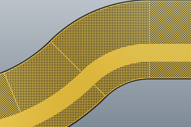
Additionally, the ribbon cable itself, or the flex cable, needs to be very flexible because it has to go over the hinge mechanism in the laptop lid. We have to ensure that we are still within our target impedance while also making sure the flex cable is flexible and won't break after a few cycles. This requires using as little copper as possible in the flex region while still hitting our target impedance, which means using a hatched reference plane. However, calculating the impedance over a hatched reference plane for those differential pairs is challenging. There is no simple equation to use; we have to go through the whole simulation process, creating a complex hatched reference plane with differential pairs above it and iteratively working out the target impedance. The simulation setup is very involved, and the mesh becomes very large.
Zach: It seems like it should be simple, just a copper grid, but when you set up a 3D simulation, it takes a long time. The same board with a solid plane goes extremely quickly.
Lukas: It gets even more complicated with bends over the hatched reference plane. If everything is aligned in parallel or perpendicular, meshing is easier. However, with curved traces above a hatched reference plane, meshing becomes very involved. You have to run a full-wave simulation with a very fine tetrahedral mesh, which can get very large depending on the simulation domain size.
Ready to start your next design project?
Our Clients and Partners


